Try the new view →
9702-2021-m-42-q05
March 2021 · Paper 42 · Question 5 · 7 marks
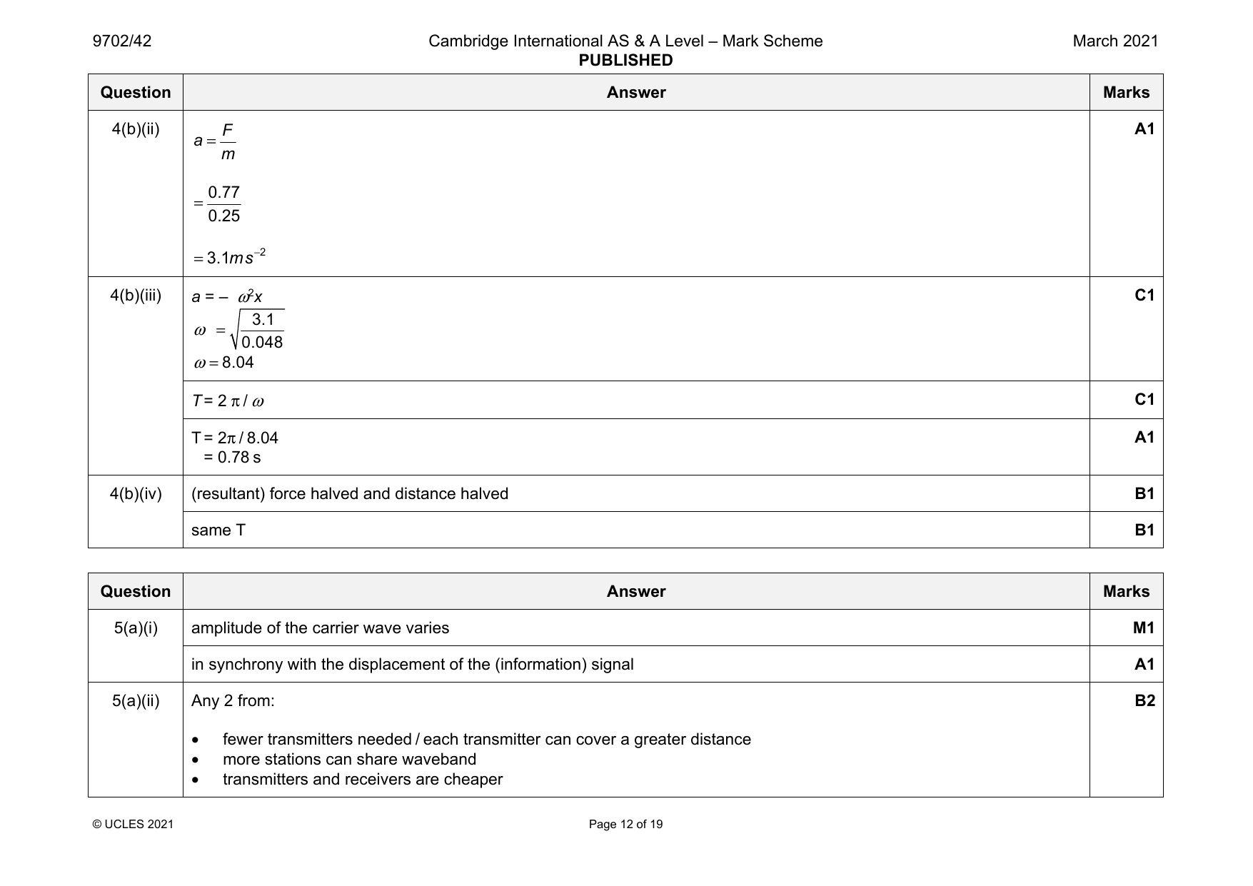
5(a)(i) amplitude of the carrier wave varies M1
in synchrony with the displacement of the (information) signal A1
5(a)(ii) Any 2 from: B2
• fewer transmitters needed / each transmitter can cover a greater distance
• more stations can share waveband
• transmitters and receivers are cheaper
© UCLES 2021 Page 12 of 19
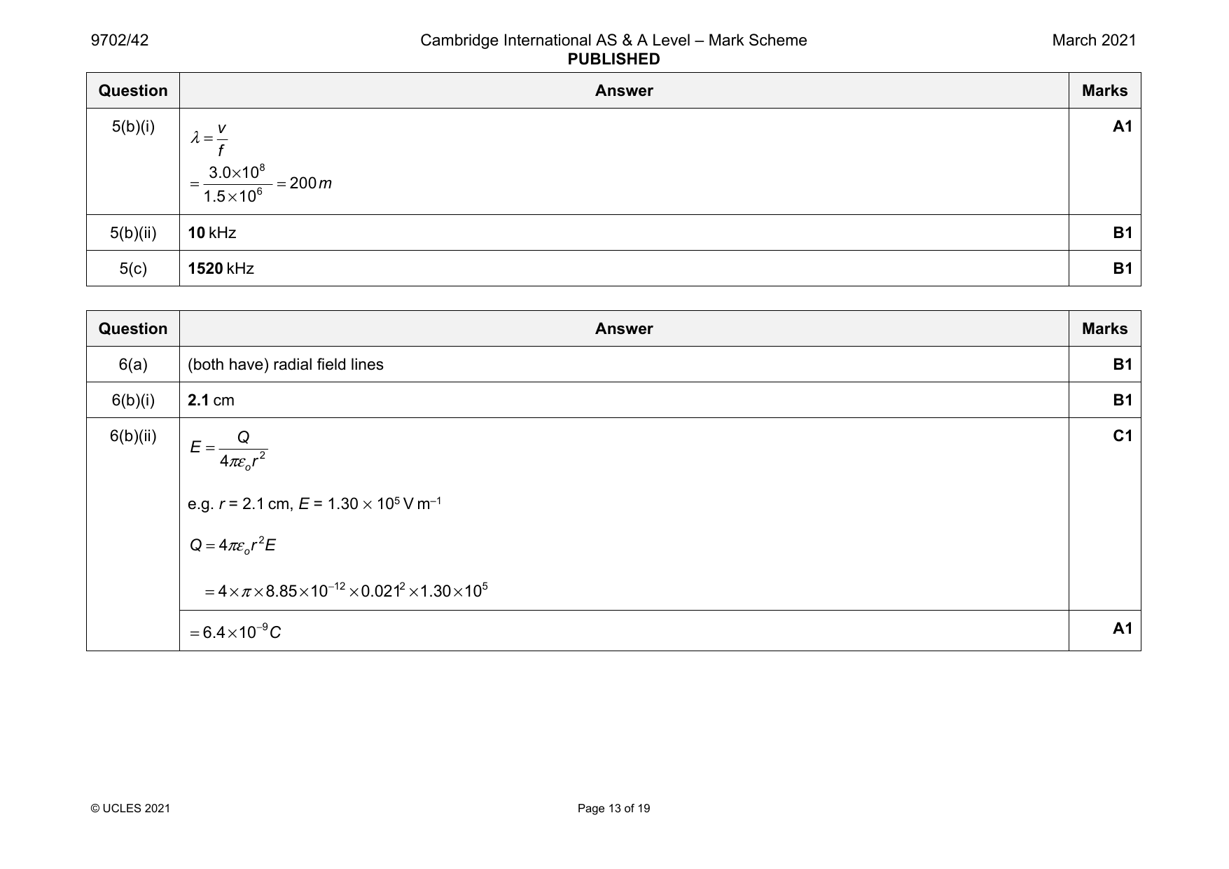
5(b)(i) v A1
λ=
f
3.0 ×108
= =200 m
1.5×10⁶
5(b)(ii) 10 kHz B1
5(c) 1520 kHz B1
Question Answer Marks
Official mark scheme pages: 12, 13 · source PDF URL
9702-2021-m-42-q07
March 2021 · Paper 42 · Question 7 · 9 marks
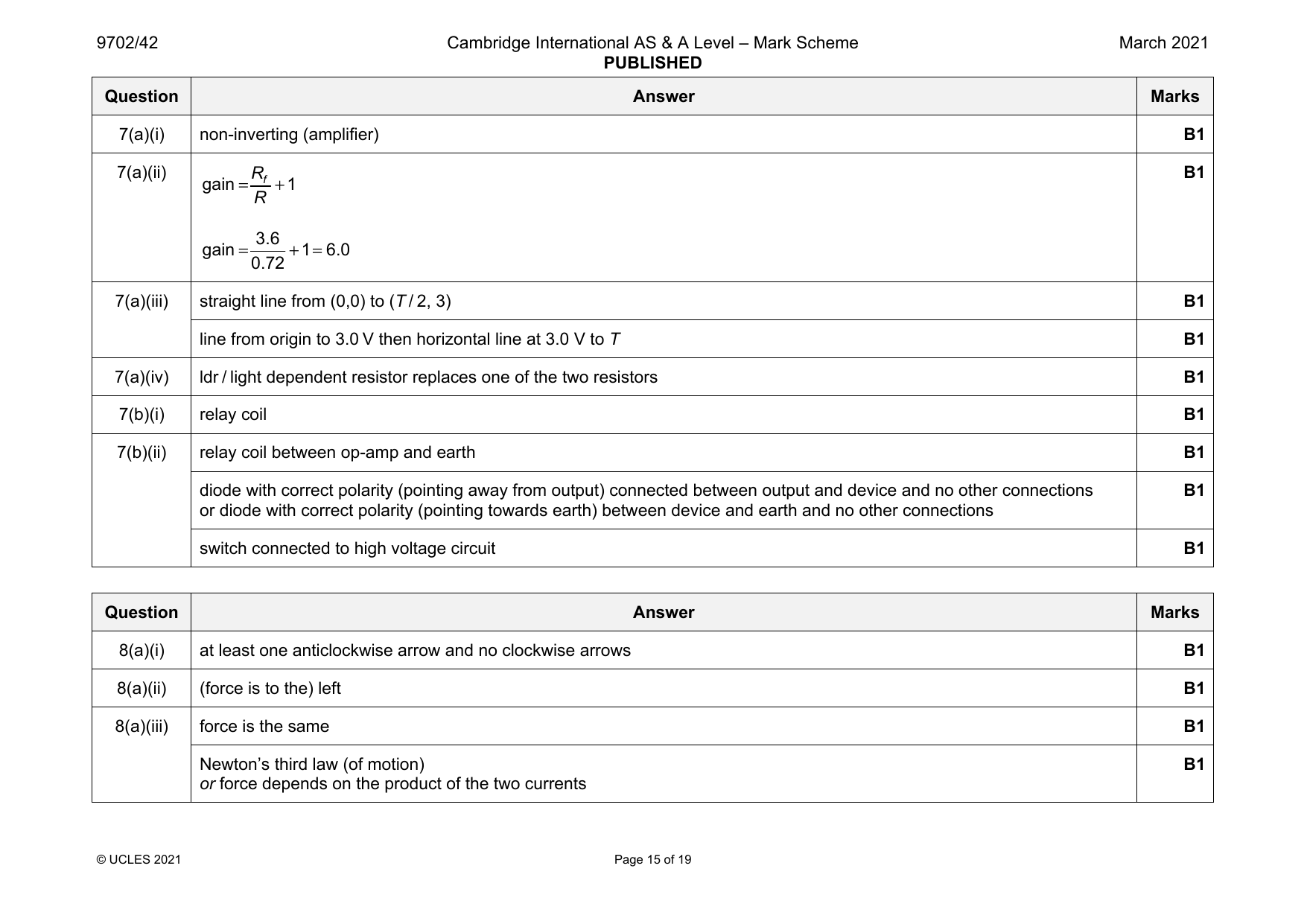
7(a)(i) non-inverting (amplifier) B1
7(a)(ii) R B1
gain= f +1
R
3.6
gain= +1=6.0
0.72
7(a)(iii) straight line from (0,0) to (T / 2, 3) B1
line from origin to 3.0 V then horizontal line at 3.0 V to T B1
7(a)(iv) ldr / light dependent resistor replaces one of the two resistors B1
7(b)(i) relay coil B1
7(b)(ii) relay coil between op-amp and earth B1
diode with correct polarity (pointing away from output) connected between output and device and no other connections B1
or diode with correct polarity (pointing towards earth) between device and earth and no other connections
switch connected to high voltage circuit B1
Question Answer Marks
Official mark scheme pages: 15 · source PDF URL
9702-2021-m-42-q10
March 2021 · Paper 42 · Question 10 · 8 marks
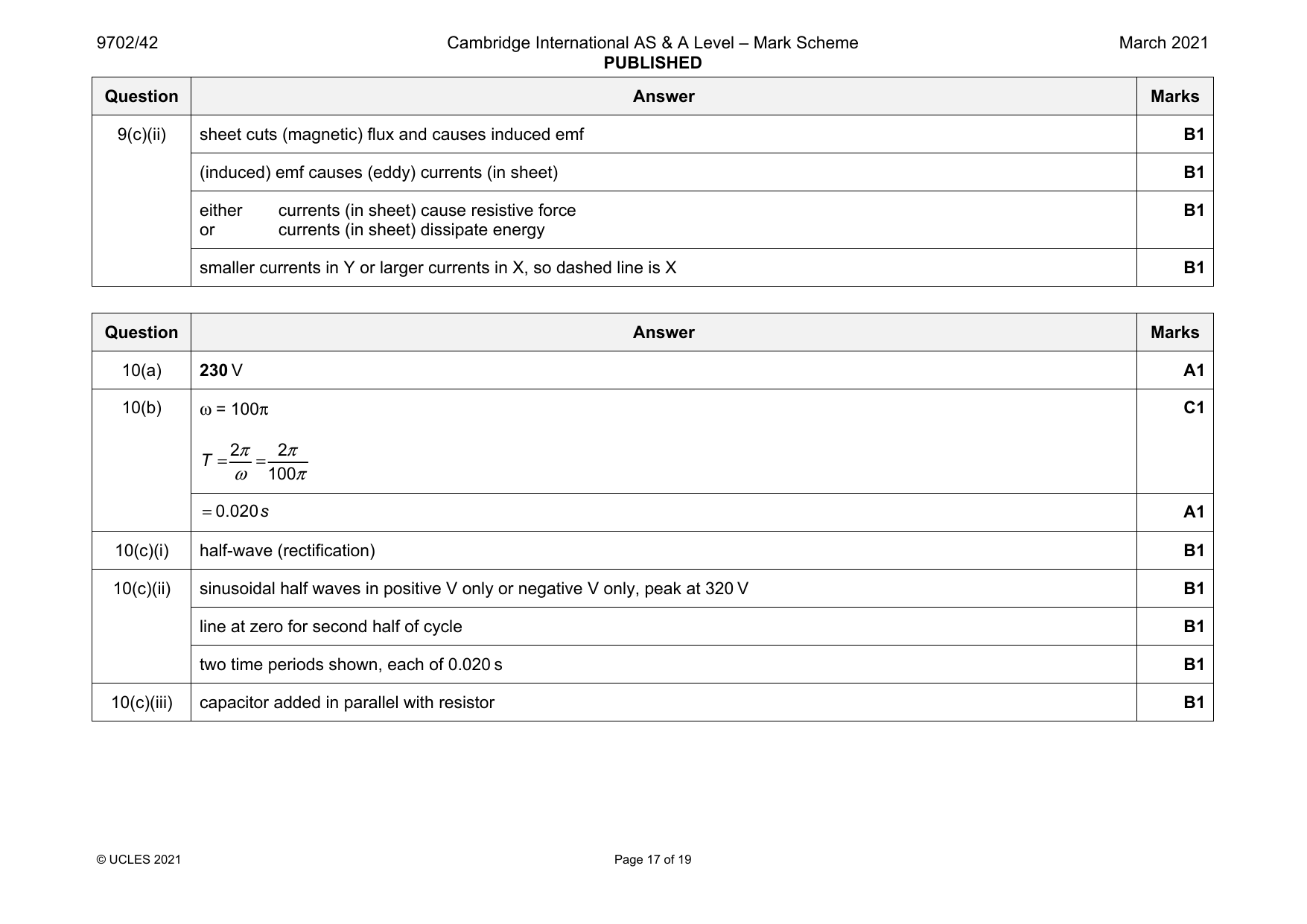
10(a) 230 V A1
10(b) ω = 100π C1
2π 2π
T = =
ω 100π
=0.020 s A1
10(c)(i) half-wave (rectification) B1
10(c)(ii) sinusoidal half waves in positive V only or negative V only, peak at 320 V B1
line at zero for second half of cycle B1
two time periods shown, each of 0.020 s B1
10(c)(iii) capacitor added in parallel with resistor B1
© UCLES 2021 Page 17 of 19
Official mark scheme pages: 17 · source PDF URL
9702-2021-mj-41-q05
May/June 2021 · Paper 41 · Question 5 · 8 marks
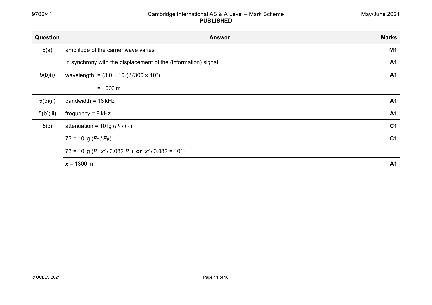
5(a) amplitude of the carrier wave varies M1
in synchrony with the displacement of the (information) signal A1
5(b)(i) wavelength = (3.0 × 10⁸) / (300 × 103) A1
= 1000 m
5(b)(ii) bandwidth = 16 kHz A1
5(b)(iii) frequency = 8 kHz A1
5(c) attenuation = 10 lg (P / P ) C1
1 2
73 = 10 lg (P / P ) C1
T R
73 = 10 lg (P x2 / 0.082 P ) or x2 / 0.082 = 107.3
T T
x = 1300 m A1
© UCLES 2021 Page 11 of 18
Official mark scheme pages: 11 · source PDF URL
9702-2021-mj-42-q04
May/June 2021 · Paper 42 · Question 4 · 8 marks
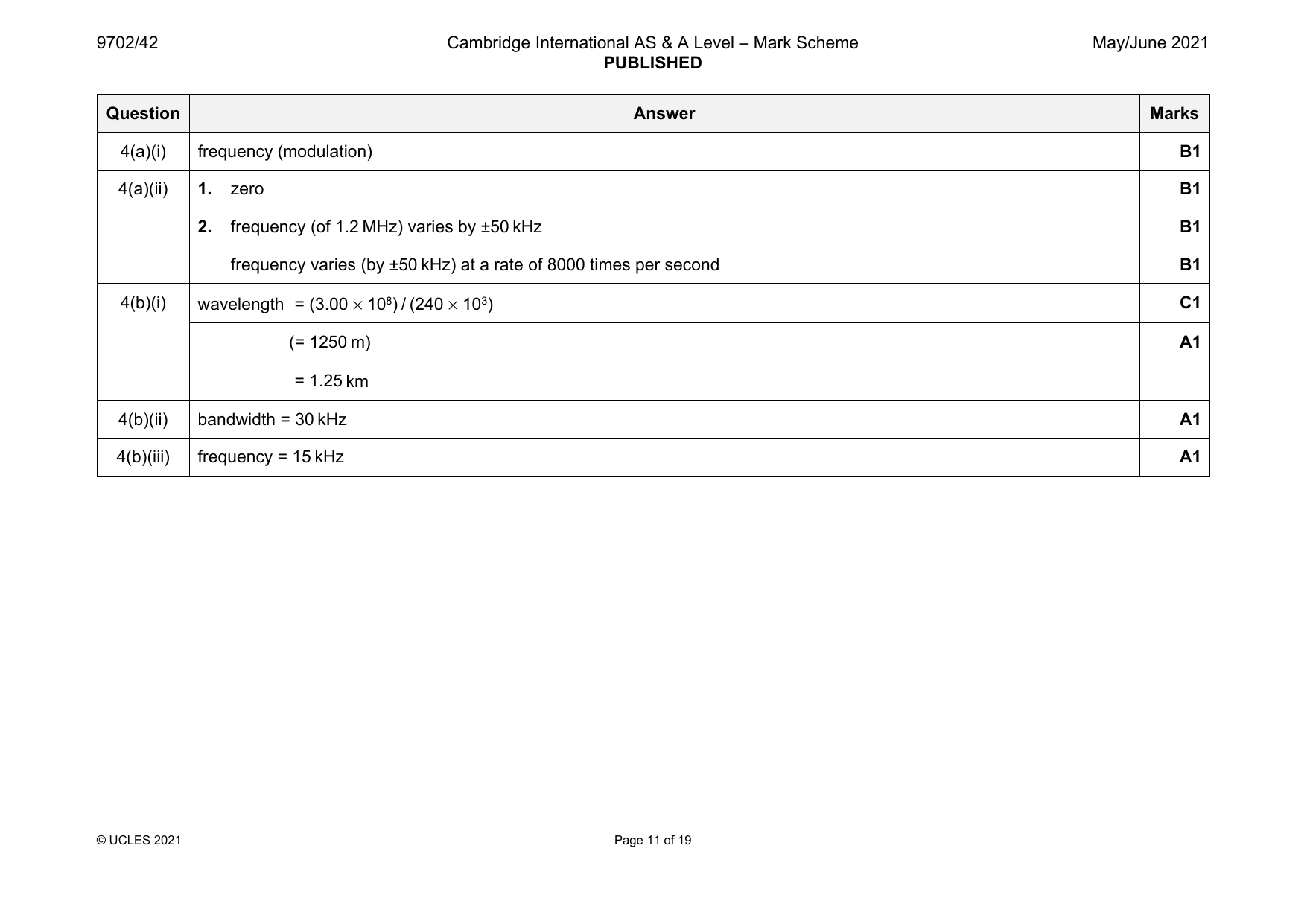
4(a)(i) frequency (modulation) B1
4(a)(ii) 1. zero B1
2. frequency (of 1.2 MHz) varies by ±50 kHz B1
frequency varies (by ±50 kHz) at a rate of 8000 times per second B1
4(b)(i) wavelength = (3.00 × 10⁸) / (240 × 103) C1
(= 1250 m) A1
= 1.25 km
4(b)(ii) bandwidth = 30 kHz A1
4(b)(iii) frequency = 15 kHz A1
© UCLES 2021 Page 11 of 19
Official mark scheme pages: 11 · source PDF URL
9702-2021-mj-42-q10
May/June 2021 · Paper 42 · Question 10 · 8 marks
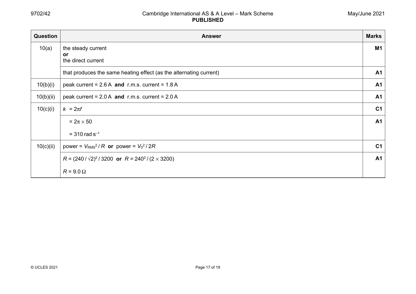
10(a) the steady current M1
or
the direct current
that produces the same heating effect (as the alternating current) A1
10(b)(i) peak current = 2.6 A and r.m.s. current = 1.8 A A1
10(b)(ii) peak current = 2.0 A and r.m.s. current = 2.0 A A1
10(c)(i) k = 2πf C1
= 2π × 50 A1
= 310 rad s–1
10(c)(ii) power = V 2 / R or power = V 2 / 2R C1
RMS 0
R = (240 / √2)2 / 3200 or R = 2402 / (2 × 3200) A1
R = 9.0 Ω
© UCLES 2021 Page 17 of 19
Official mark scheme pages: 17 · source PDF URL
9702-2021-mj-43-q05
May/June 2021 · Paper 43 · Question 5 · 8 marks
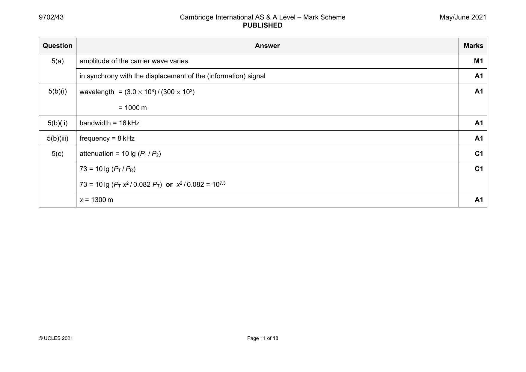
5(a) amplitude of the carrier wave varies M1
in synchrony with the displacement of the (information) signal A1
5(b)(i) wavelength = (3.0 × 10⁸) / (300 × 103) A1
= 1000 m
5(b)(ii) bandwidth = 16 kHz A1
5(b)(iii) frequency = 8 kHz A1
5(c) attenuation = 10 lg (P / P ) C1
1 2
73 = 10 lg (P / P ) C1
T R
73 = 10 lg (P x2 / 0.082 P ) or x2 / 0.082 = 107.3
T T
x = 1300 m A1
© UCLES 2021 Page 11 of 18
Official mark scheme pages: 11 · source PDF URL
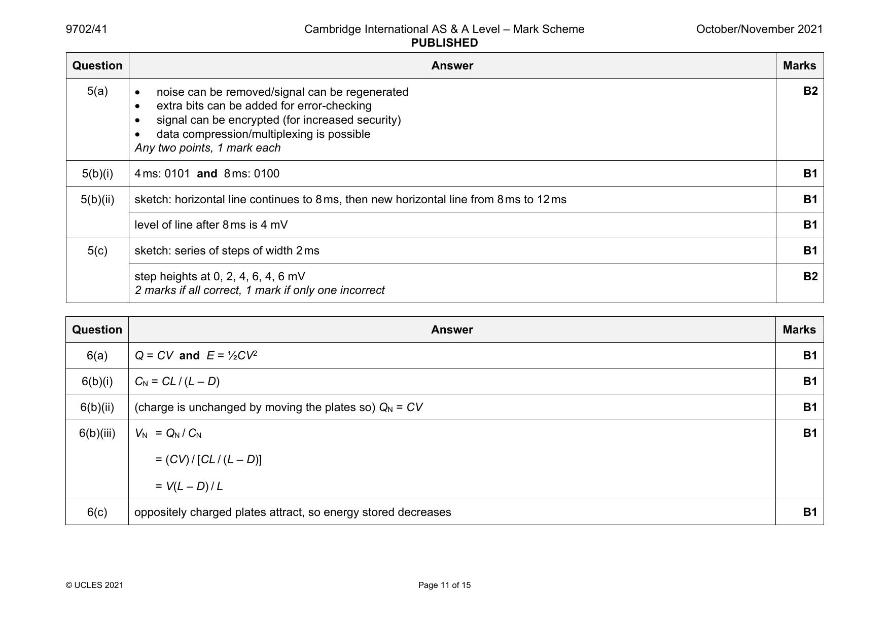
9702-2021-on-41-q05
Oct/Nov 2021 · Paper 41 · Question 5 · 8 marks
5(a) • noise can be removed/signal can be regenerated B2
• extra bits can be added for error-checking
• signal can be encrypted (for increased security)
• data compression/multiplexing is possible
Any two points, 1 mark each
5(b)(i) 4ms: 0101 and 8ms: 0100 B1
5(b)(ii) sketch: horizontal line continues to 8ms, then new horizontal line from 8ms to 12ms B1
level of line after 8ms is 4 mV B1
5(c) sketch: series of steps of width 2ms B1
step heights at 0, 2, 4, 6, 4, 6 mV B2
2 marks if all correct, 1 mark if only one incorrect
Question Answer Marks
Official mark scheme pages: 11 · source PDF URL
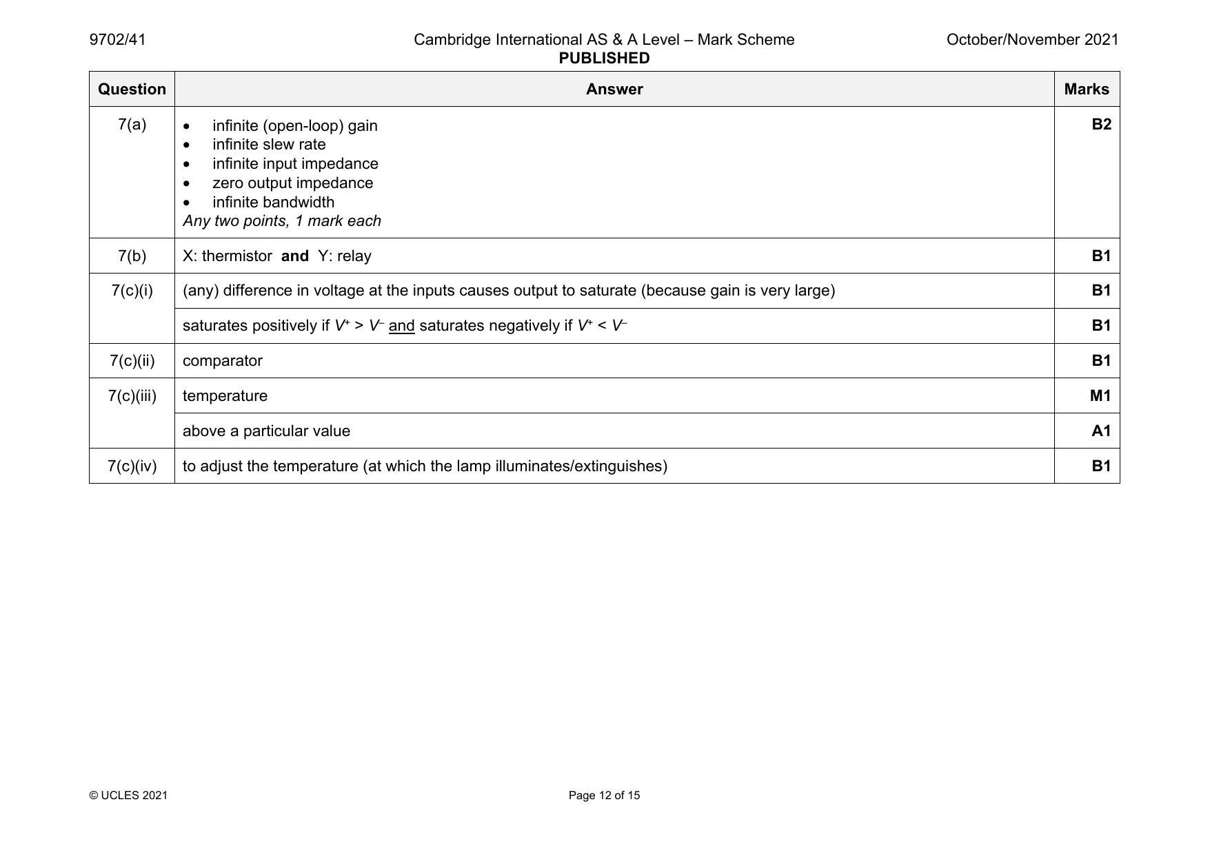
9702-2021-on-41-q07
Oct/Nov 2021 · Paper 41 · Question 7 · 9 marks
7(a) • infinite (open-loop) gain B2
• infinite slew rate
• infinite input impedance
• zero output impedance
• infinite bandwidth
Any two points, 1 mark each
7(b) X: thermistor and Y: relay B1
7(c)(i) (any) difference in voltage at the inputs causes output to saturate (because gain is very large) B1
saturates positively if V+ > V– and saturates negatively if V+ < V– B1
7(c)(ii) comparator B1
7(c)(iii) temperature M1
above a particular value A1
7(c)(iv) to adjust the temperature (at which the lamp illuminates/extinguishes) B1
© UCLES 2021 Page 12 of 15
Official mark scheme pages: 12 · source PDF URL
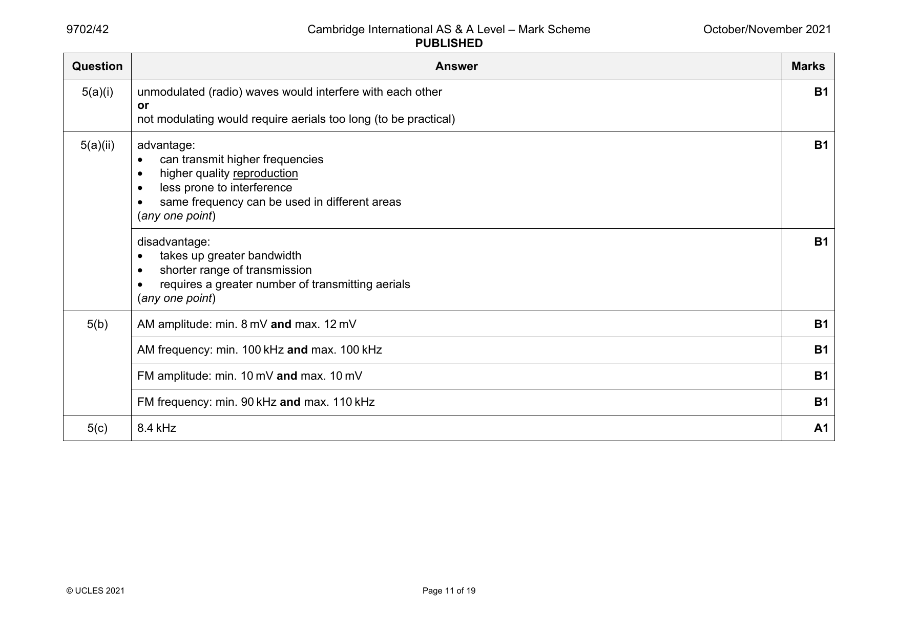
9702-2021-on-42-q05
Oct/Nov 2021 · Paper 42 · Question 5 · 8 marks
5(a)(i) unmodulated (radio) waves would interfere with each other B1
or
not modulating would require aerials too long (to be practical)
5(a)(ii) advantage: B1
• can transmit higher frequencies
• higher quality reproduction
• less prone to interference
• same frequency can be used in different areas
(any one point)
disadvantage: B1
• takes up greater bandwidth
• shorter range of transmission
• requires a greater number of transmitting aerials
(any one point)
5(b) AM amplitude: min. 8 mV and max. 12 mV B1
AM frequency: min. 100 kHz and max. 100 kHz B1
FM amplitude: min. 10 mV and max. 10 mV B1
FM frequency: min. 90 kHz and max. 110 kHz B1
5(c) 8.4 kHz A1
© UCLES 2021 Page 11 of 19
Official mark scheme pages: 11 · source PDF URL
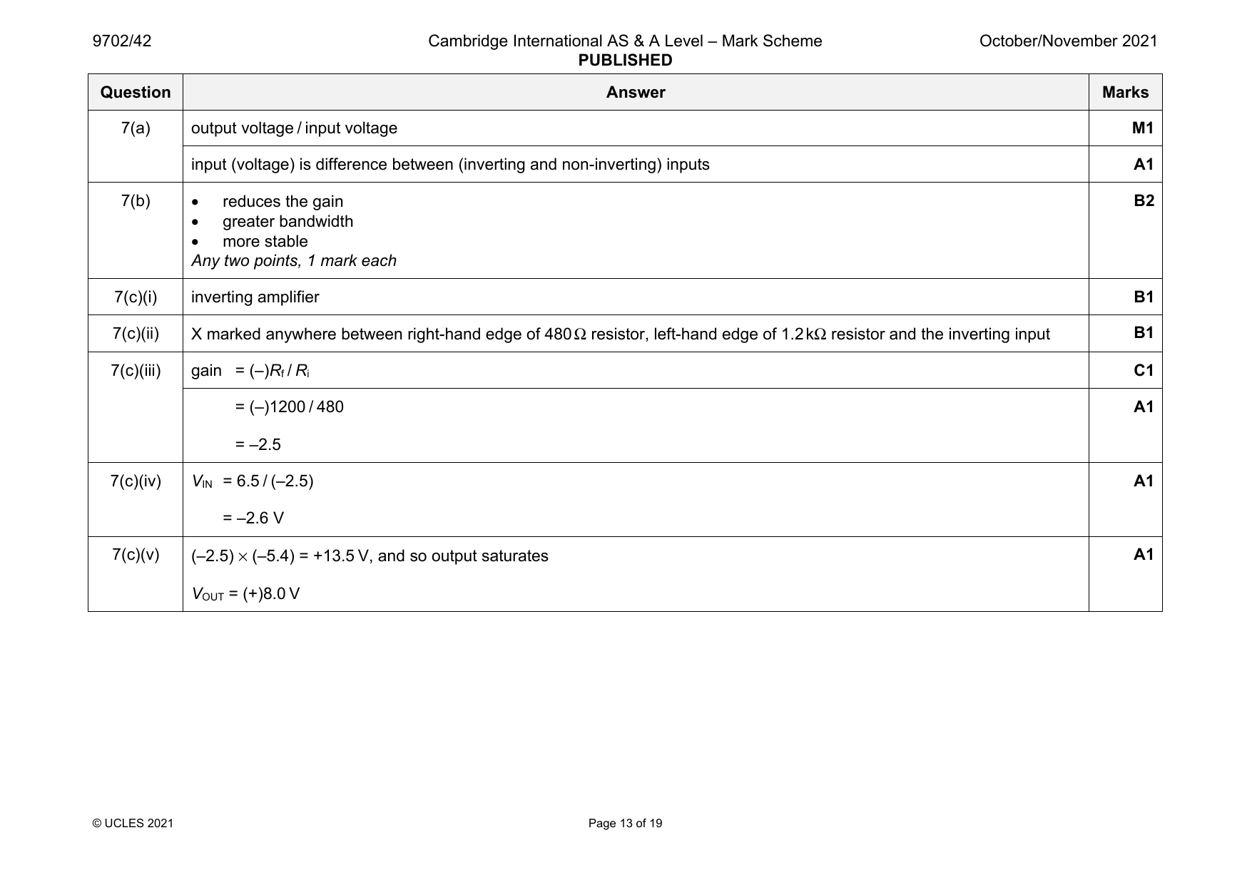
9702-2021-on-42-q07
Oct/Nov 2021 · Paper 42 · Question 7 · 10 marks
7(a) output voltage / input voltage M1
input (voltage) is difference between (inverting and non-inverting) inputs A1
7(b) • reduces the gain B2
• greater bandwidth
• more stable
Any two points, 1 mark each
7(c)(i) inverting amplifier B1
7(c)(ii) X marked anywhere between right-hand edge of 480Ω resistor, left-hand edge of 1.2kΩ resistor and the inverting input B1
7(c)(iii) gain = (–)R / R C1
f i
= (–)1200 / 480 A1
= –2.5
7(c)(iv) V = 6.5 / (–2.5) A1
IN
= –2.6 V
7(c)(v) (–2.5) × (–5.4) = +13.5 V, and so output saturates A1
V = (+)8.0 V
OUT
© UCLES 2021 Page 13 of 19
Official mark scheme pages: 13 · source PDF URL
9702-2021-on-42-q10
Oct/Nov 2021 · Paper 42 · Question 10 · 10 marks
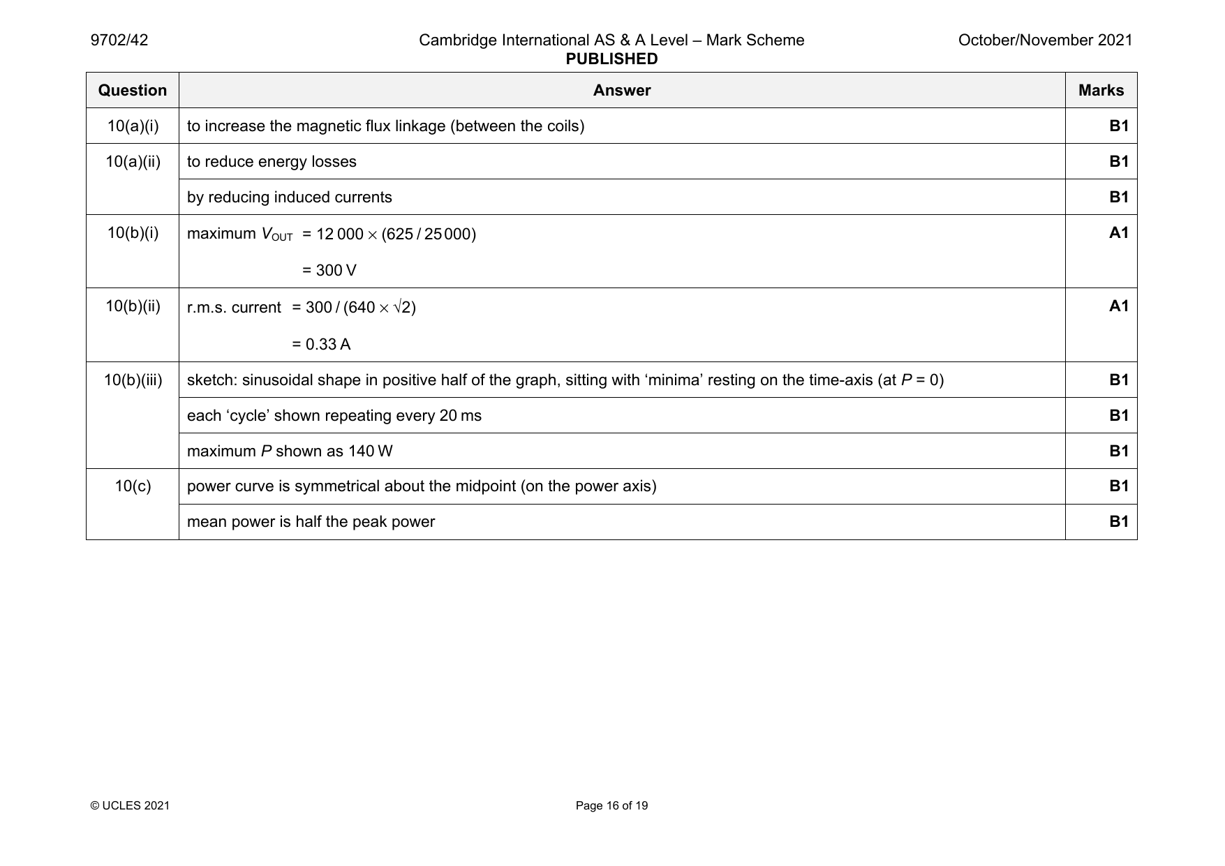
10(a)(i) to increase the magnetic flux linkage (between the coils) B1
10(a)(ii) to reduce energy losses B1
by reducing induced currents B1
10(b)(i) maximum V = 12 000 × (625 / 25000) A1
OUT
= 300 V
10(b)(ii) r.m.s. current = 300 / (640 × √2) A1
= 0.33 A
10(b)(iii) sketch: sinusoidal shape in positive half of the graph, sitting with ‘minima’ resting on the time-axis (at P = 0) B1
each ‘cycle’ shown repeating every 20 ms B1
maximum P shown as 140 W B1
10(c) power curve is symmetrical about the midpoint (on the power axis) B1
mean power is half the peak power B1
© UCLES 2021 Page 16 of 19
Official mark scheme pages: 16 · source PDF URL
9702-2021-on-43-q05
Oct/Nov 2021 · Paper 43 · Question 5 · 8 marks
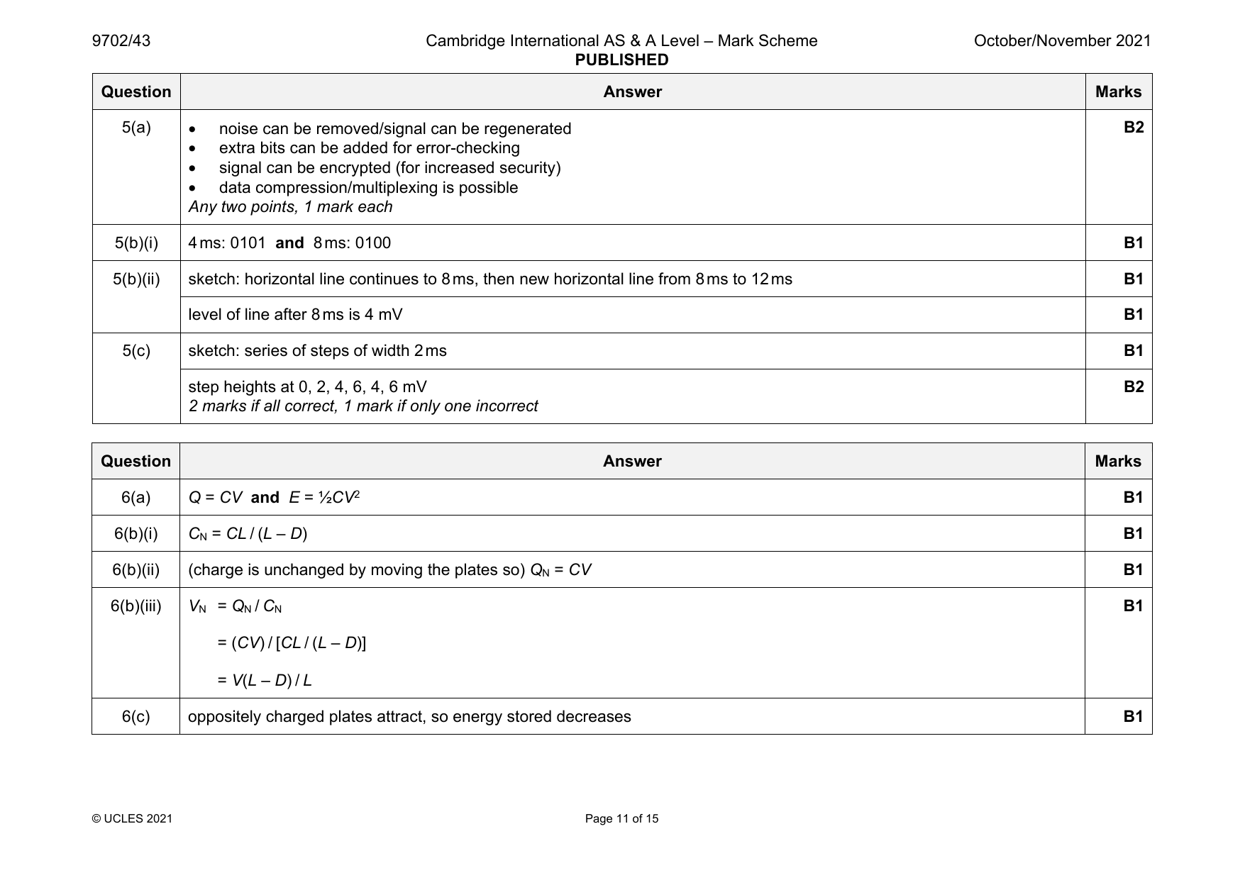
5(a) • noise can be removed/signal can be regenerated B2
• extra bits can be added for error-checking
• signal can be encrypted (for increased security)
• data compression/multiplexing is possible
Any two points, 1 mark each
5(b)(i) 4ms: 0101 and 8ms: 0100 B1
5(b)(ii) sketch: horizontal line continues to 8ms, then new horizontal line from 8ms to 12ms B1
level of line after 8ms is 4 mV B1
5(c) sketch: series of steps of width 2ms B1
step heights at 0, 2, 4, 6, 4, 6 mV B2
2 marks if all correct, 1 mark if only one incorrect
Question Answer Marks
Official mark scheme pages: 11 · source PDF URL
9702-2021-on-43-q07
Oct/Nov 2021 · Paper 43 · Question 7 · 9 marks
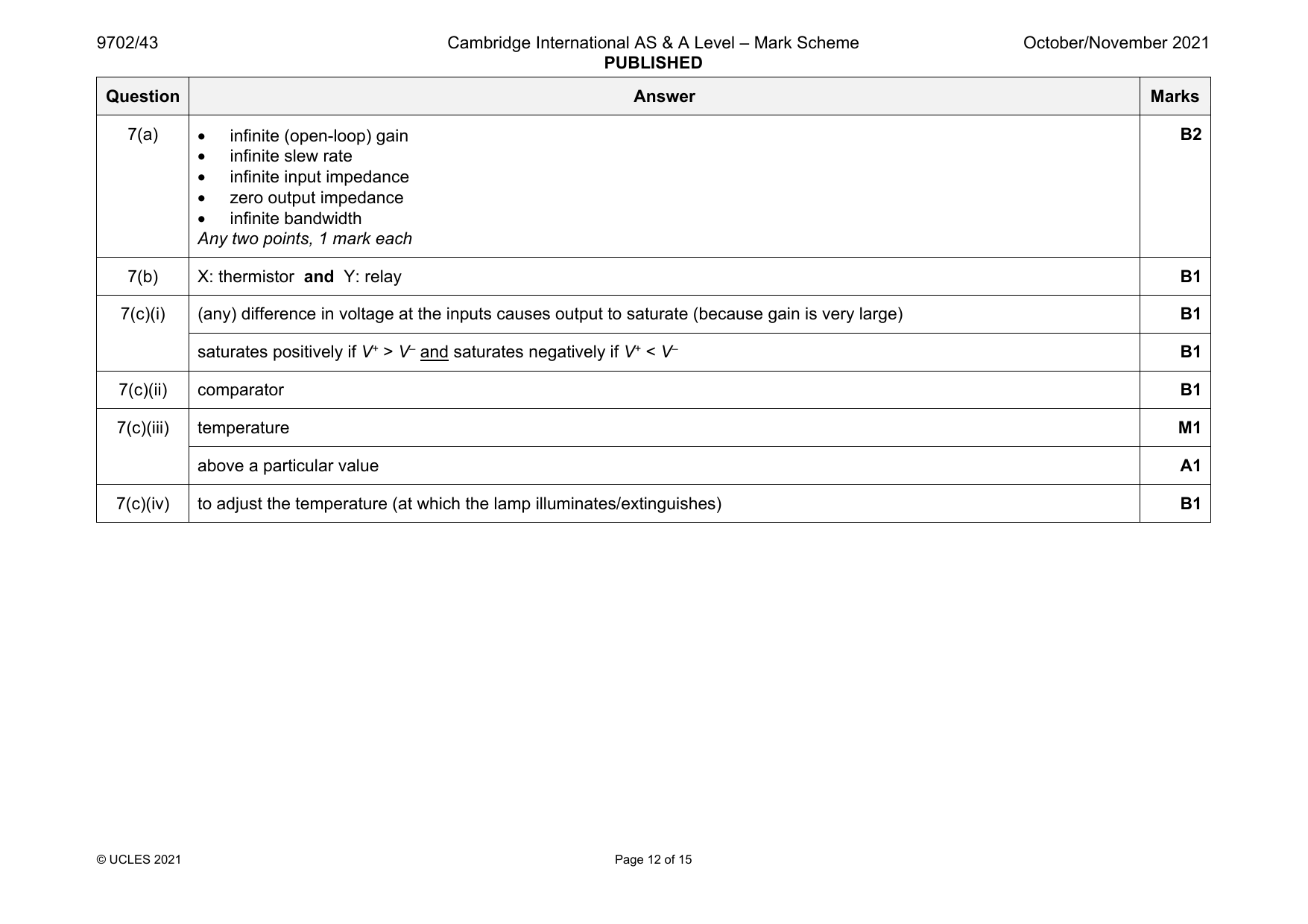
7(a) • infinite (open-loop) gain B2
• infinite slew rate
• infinite input impedance
• zero output impedance
• infinite bandwidth
Any two points, 1 mark each
7(b) X: thermistor and Y: relay B1
7(c)(i) (any) difference in voltage at the inputs causes output to saturate (because gain is very large) B1
saturates positively if V+ > V– and saturates negatively if V+ < V– B1
7(c)(ii) comparator B1
7(c)(iii) temperature M1
above a particular value A1
7(c)(iv) to adjust the temperature (at which the lamp illuminates/extinguishes) B1
© UCLES 2021 Page 12 of 15
Official mark scheme pages: 12 · source PDF URL
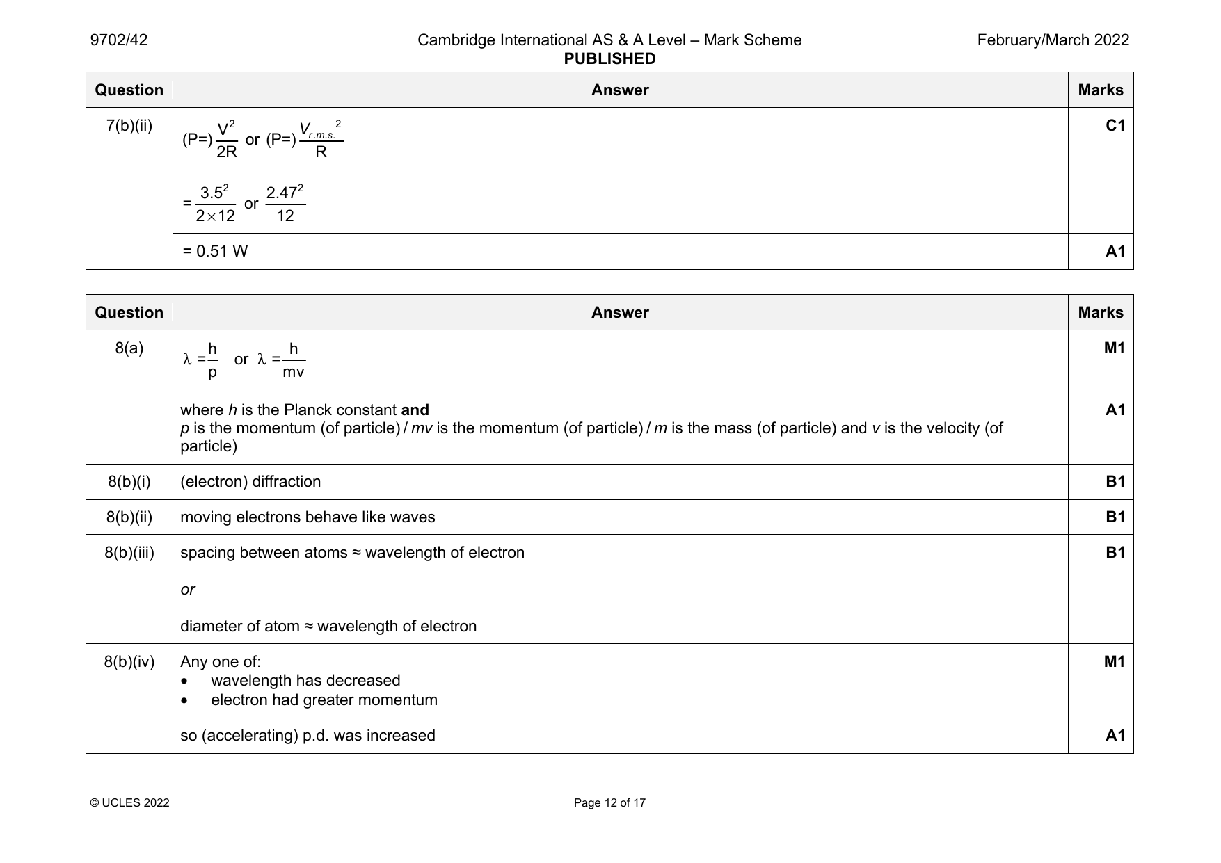
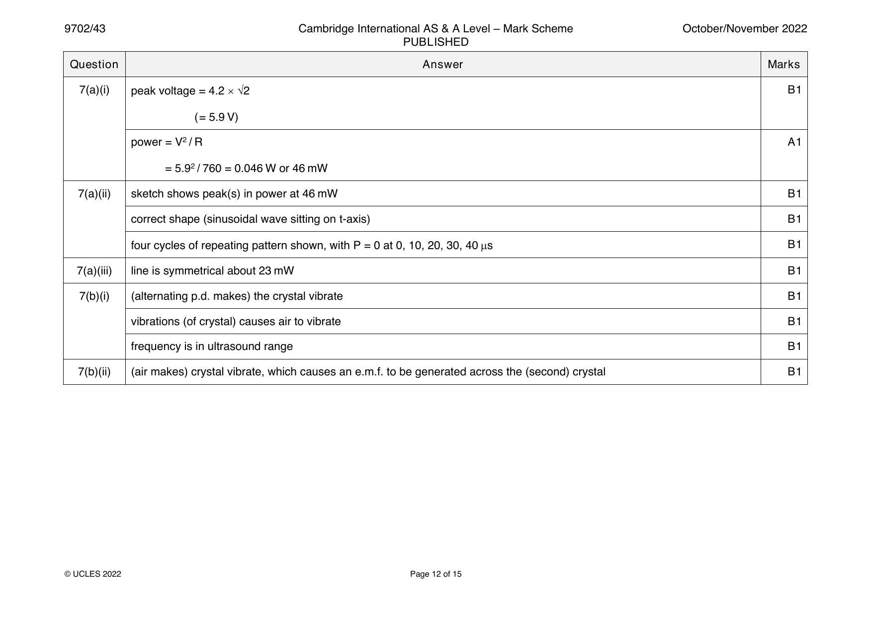
9702-2022-m-42-q07
March 2022 · Paper 42 · Question 7 · 6 marks
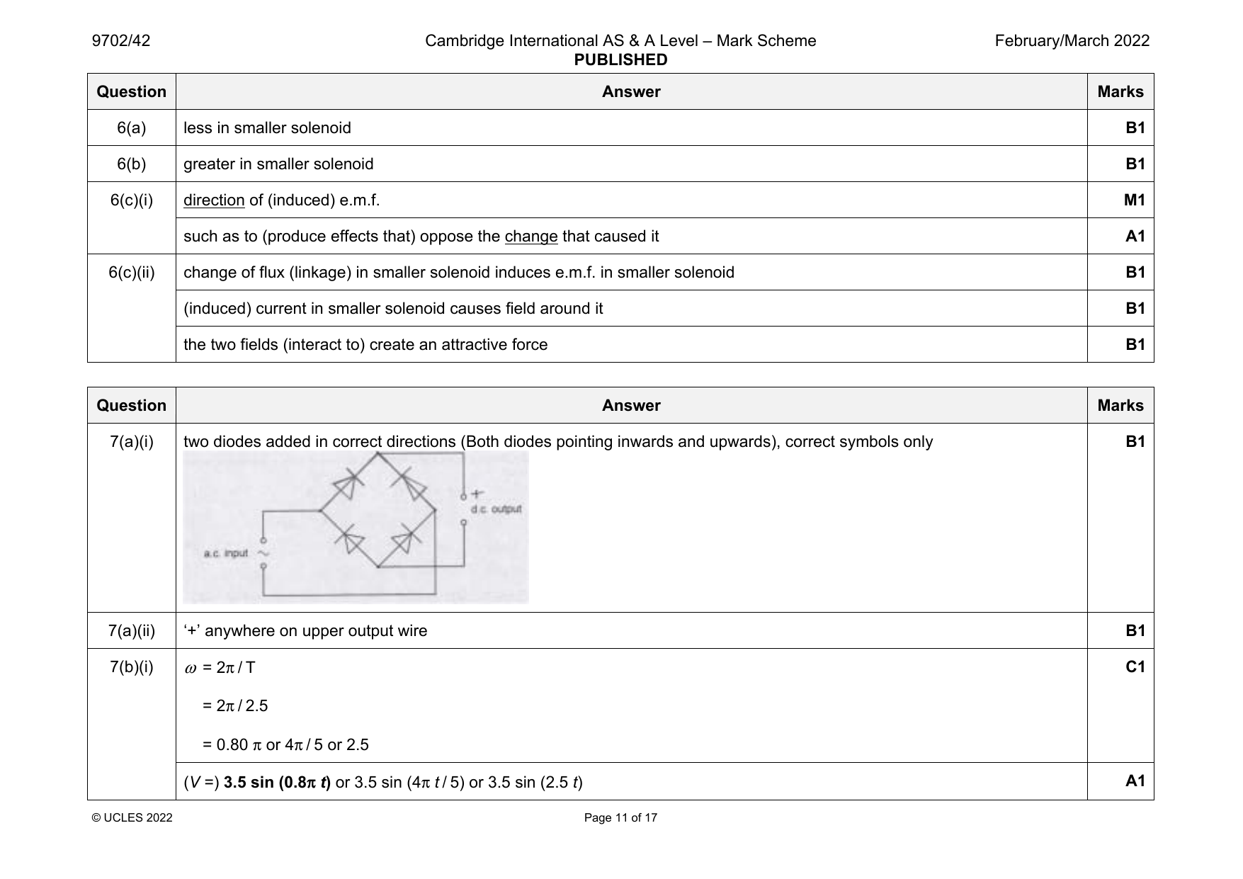
7(a)(i) two diodes added in correct directions (Both diodes pointing inwards and upwards), correct symbols only B1
7(a)(ii) ‘+’ anywhere on upper output wire B1
7(b)(i) ω = 2π / T C1
= 2π / 2.5
= 0.80 π or 4π / 5 or 2.5
(V =) 3.5 sin (0.8π t) or 3.5 sin (4π t / 5) or 3.5 sin (2.5 t) A1
© UCLES 2022 Page 11 of 17
7(b)(ii) V2 V 2 C1
(P=) or (P=) r.m.s.
2R R
3.52 2.472
= or
2×12 12
= 0.51 W A1
Question Answer Marks
Official mark scheme pages: 11, 12 · source PDF URL
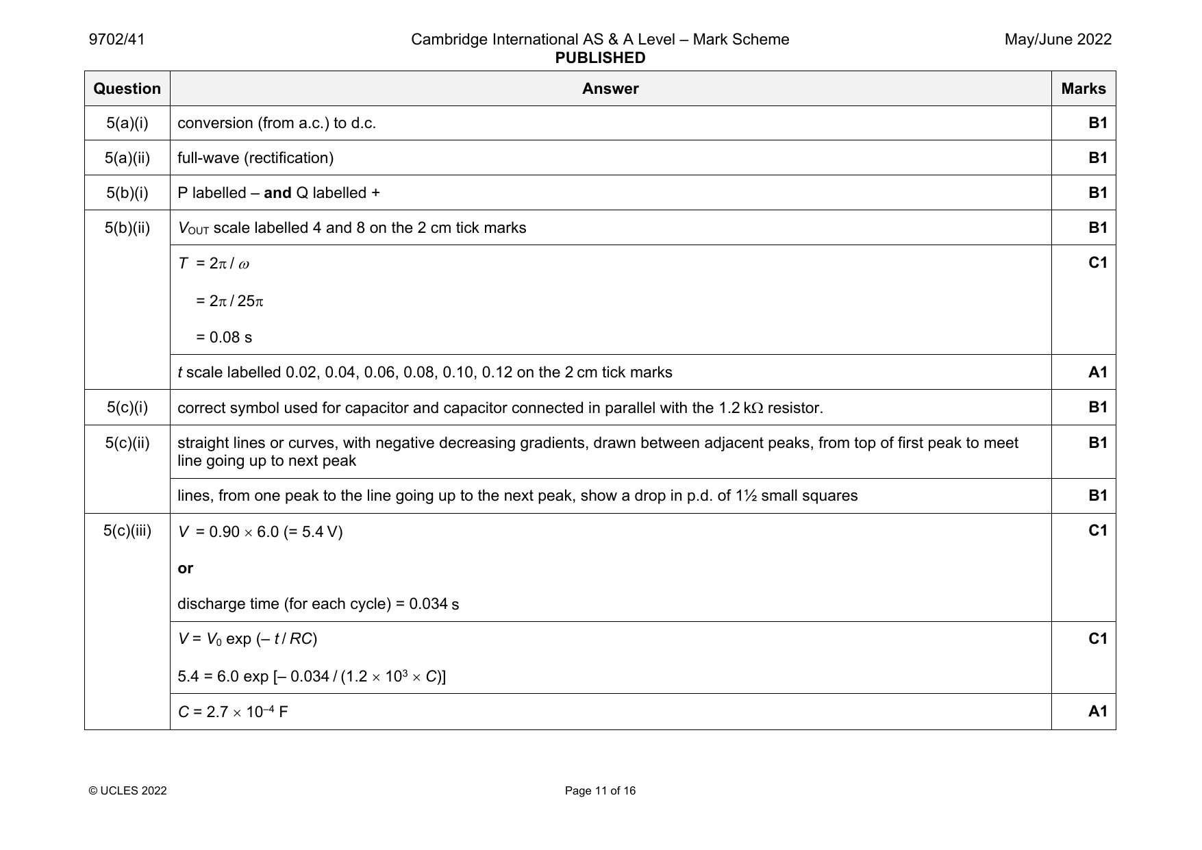
9702-2022-mj-41-q05
May/June 2022 · Paper 41 · Question 5 · 12 marks
5(a)(i) conversion (from a.c.) to d.c. B1
5(a)(ii) full-wave (rectification) B1
5(b)(i) P labelled – and Q labelled + B1
5(b)(ii) V scale labelled 4 and 8 on the 2 cm tick marks B1
OUT
T = 2 / C1
= 2 / 25
= 0.08 s
t scale labelled 0.02, 0.04, 0.06, 0.08, 0.10, 0.12 on the 2 cm tick marks A1
5(c)(i) correct symbol used for capacitor and capacitor connected in parallel with the 1.2 k resistor. B1
5(c)(ii) straight lines or curves, with negative decreasing gradients, drawn between adjacent peaks, from top of first peak to meet B1
line going up to next peak
lines, from one peak to the line going up to the next peak, show a drop in p.d. of 1½ small squares B1
5(c)(iii) V = 0.90 6.0 (= 5.4 V) C1
or
discharge time (for each cycle) = 0.034 s
V = V exp (– t / RC) C1
0
5.4 = 6.0 exp [– 0.034 / (1.2 103 C)]
C = 2.7 10–4 F A1
© UCLES 2022 Page 11 of 16
Official mark scheme pages: 11 · source PDF URL
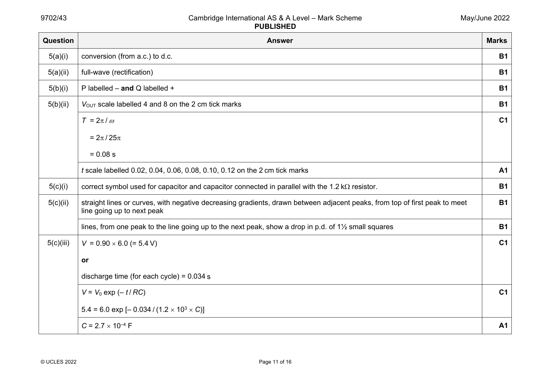
9702-2022-mj-43-q05
May/June 2022 · Paper 43 · Question 5 · 12 marks
5(a)(i) conversion (from a.c.) to d.c. B1
5(a)(ii) full-wave (rectification) B1
5(b)(i) P labelled – and Q labelled + B1
5(b)(ii) V scale labelled 4 and 8 on the 2 cm tick marks B1
OUT
T = 2 / C1
= 2 / 25
= 0.08 s
t scale labelled 0.02, 0.04, 0.06, 0.08, 0.10, 0.12 on the 2 cm tick marks A1
5(c)(i) correct symbol used for capacitor and capacitor connected in parallel with the 1.2 k resistor. B1
5(c)(ii) straight lines or curves, with negative decreasing gradients, drawn between adjacent peaks, from top of first peak to meet B1
line going up to next peak
lines, from one peak to the line going up to the next peak, show a drop in p.d. of 1½ small squares B1
5(c)(iii) V = 0.90 6.0 (= 5.4 V) C1
or
discharge time (for each cycle) = 0.034 s
V = V exp (– t / RC) C1
0
5.4 = 6.0 exp [– 0.034 / (1.2 103 C)]
C = 2.7 10–4 F A1
© UCLES 2022 Page 11 of 16
Official mark scheme pages: 11 · source PDF URL
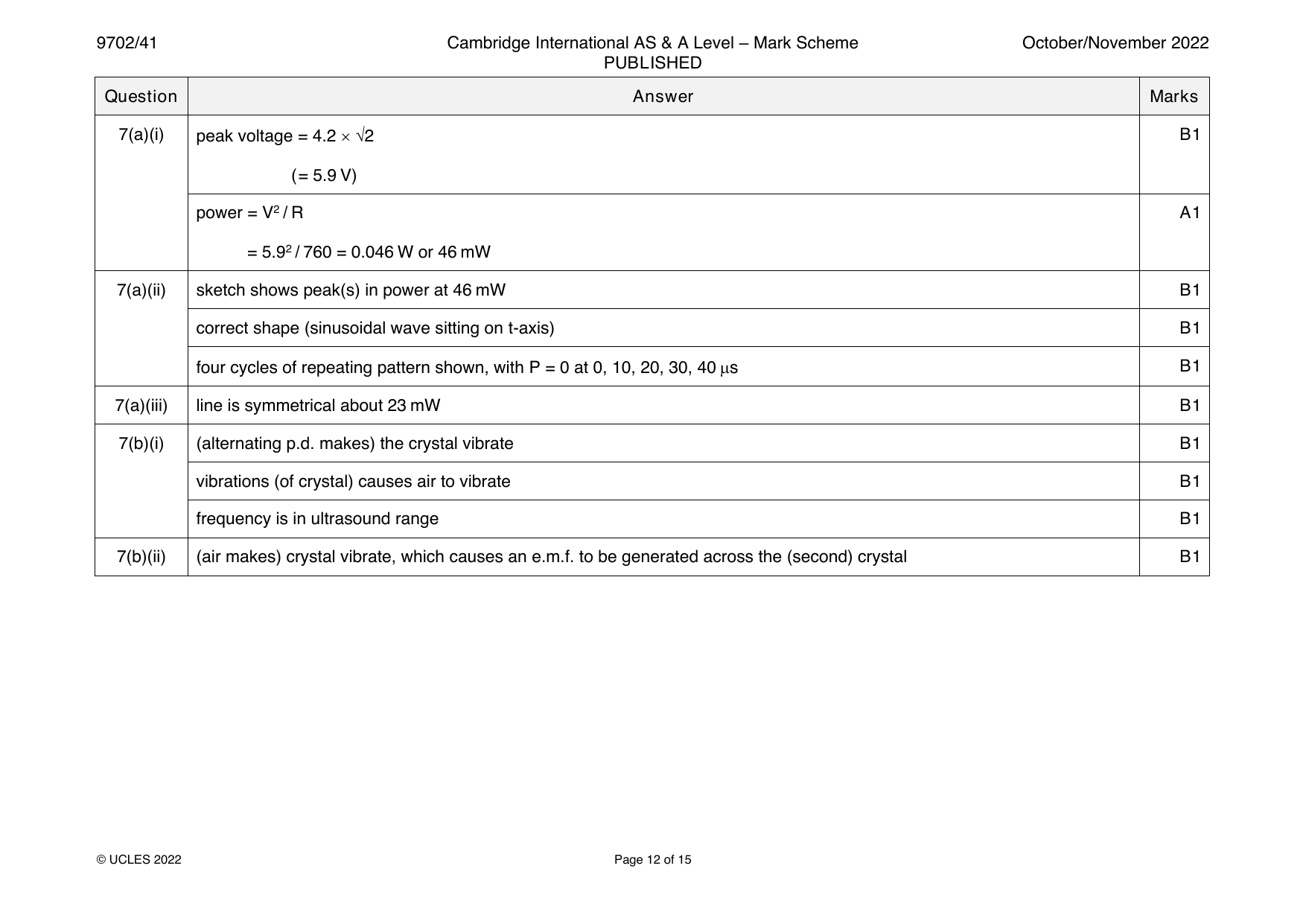
9702-2022-on-41-q07
Oct/Nov 2022 · Paper 41 · Question 7 · 10 marks
7(a)(i) peak voltage = 4.2 2 B1
( = 5.9 V)
power = V2 / R A1
= 5.92 / 760 = 0.046 W or 46 mW
7(a)(ii) sketch shows peak(s) in power at 46 mW B1
correct shape (sinusoidal wave sitting on t-axis) B1
four cycles of repeating pattern shown, with P = 0 at 0, 10, 20, 30, 40 s B1
7(a)(iii) line is symmetrical about 23 mW B1
7(b)(i) (alternating p.d. makes) the crystal vibrate B1
vibrations (of crystal) causes air to vibrate B1
frequency is in ultrasound range B1
7(b)(ii) (air makes) crystal vibrate, which causes an e.m.f. to be generated across the (second) crystal B1
© UCLES 2022 Page 12 of 15
Official mark scheme pages: 12 · source PDF URL
9702-2022-on-43-q07
Oct/Nov 2022 · Paper 43 · Question 7 · 10 marks
7(a)(i) peak voltage = 4.2 2 B1
( = 5.9 V)
power = V2 / R A1
= 5.92 / 760 = 0.046 W or 46 mW
7(a)(ii) sketch shows peak(s) in power at 46 mW B1
correct shape (sinusoidal wave sitting on t-axis) B1
four cycles of repeating pattern shown, with P = 0 at 0, 10, 20, 30, 40 s B1
7(a)(iii) line is symmetrical about 23 mW B1
7(b)(i) (alternating p.d. makes) the crystal vibrate B1
vibrations (of crystal) causes air to vibrate B1
frequency is in ultrasound range B1
7(b)(ii) (air makes) crystal vibrate, which causes an e.m.f. to be generated across the (second) crystal B1
© UCLES 2022 Page 12 of 15
Official mark scheme pages: 12 · source PDF URL
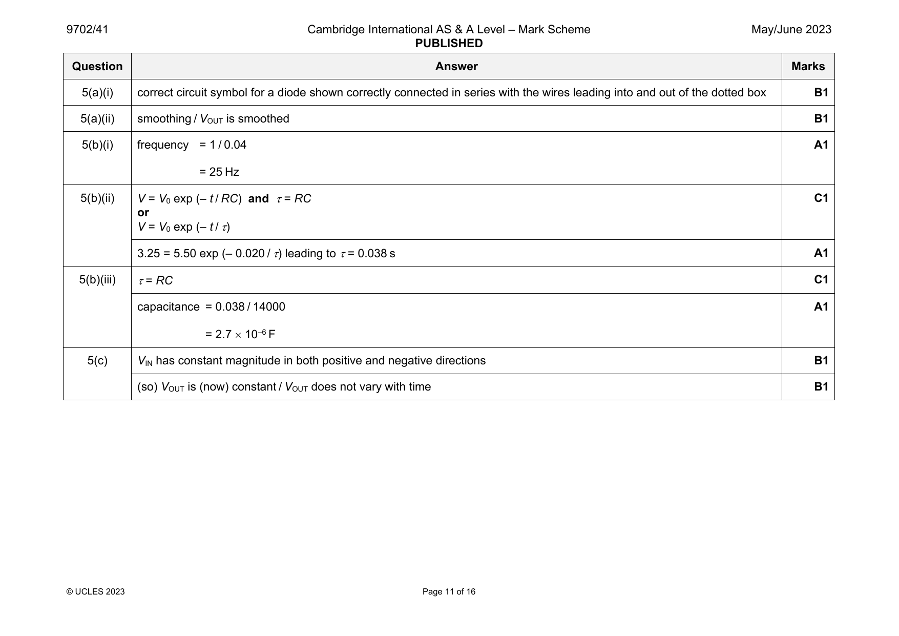
9702-2023-mj-41-q05
May/June 2023 · Paper 41 · Question 5 · 9 marks
5(a)(i) correct circuit symbol for a diode shown correctly connected in series with the wires leading into and out of the dotted box B1
5(a)(ii) smoothing / V is smoothed B1
OUT
5(b)(i) frequency = 1 / 0.04 A1
= 25 Hz
5(b)(ii) V = V exp (– t / RC) and = RC C1
0
or
V = V exp (– t / )
0
3.25 = 5.50 exp (– 0.020 / ) leading to = 0.038 s A1
5(b)(iii) = RC C1
capacitance = 0.038 / 14000 A1
= 2.7 10–6 F
5(c) V has constant magnitude in both positive and negative directions B1
IN
(so) V is (now) constant / V does not vary with time B1
OUT OUT
© UCLES 2023 Page 11 of 16
Official mark scheme pages: 11 · source PDF URL
9702-2023-mj-42-q07
May/June 2023 · Paper 42 · Question 7 · 10 marks
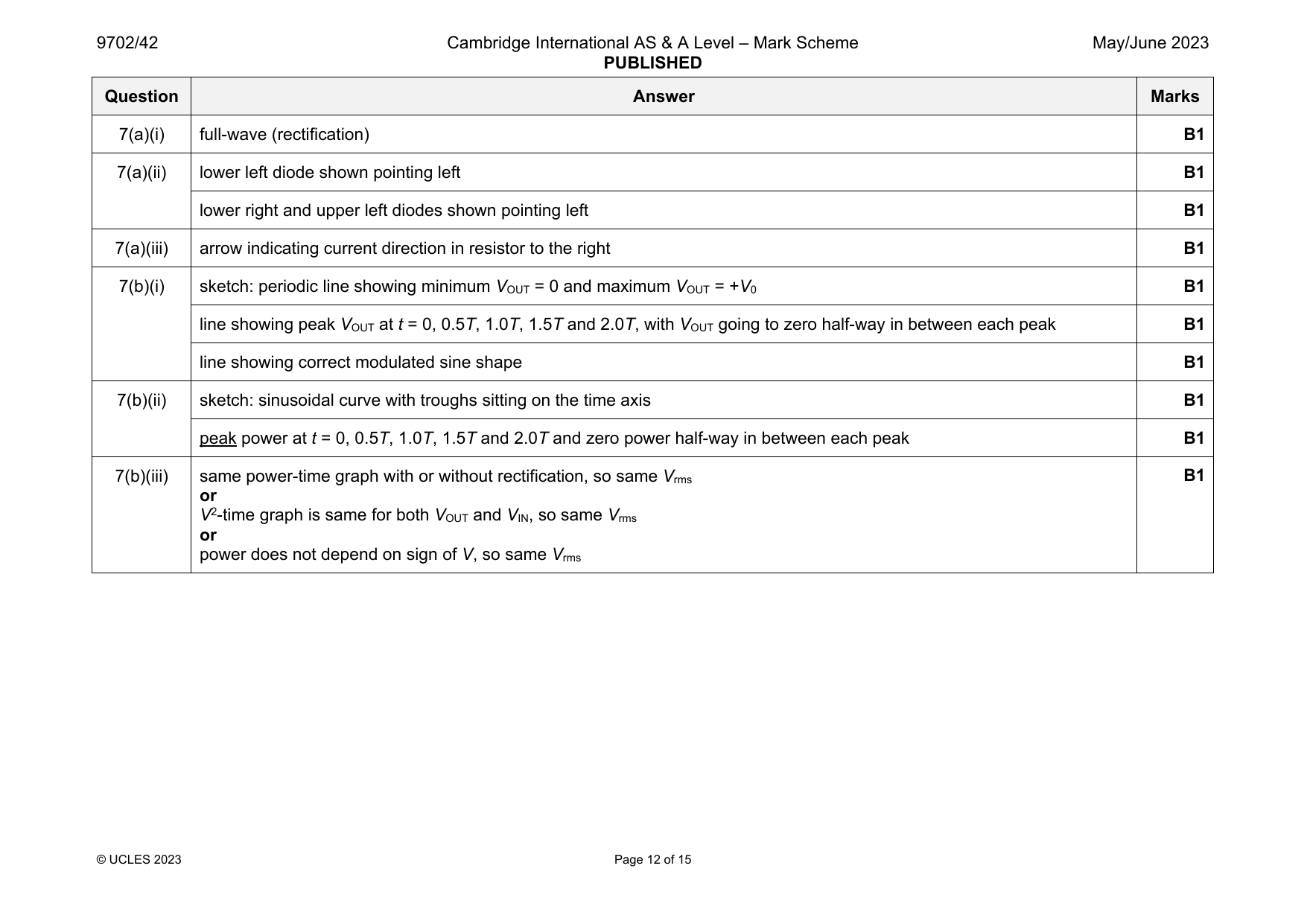
7(a)(i) full-wave (rectification) B1
7(a)(ii) lower left diode shown pointing left B1
lower right and upper left diodes shown pointing left B1
7(a)(iii) arrow indicating current direction in resistor to the right B1
7(b)(i) sketch: periodic line showing minimum V = 0 and maximum V = +V B1
OUT OUT 0
line showing peak V at t = 0, 0.5T, 1.0T, 1.5T and 2.0T, with V going to zero half-way in between each peak B1
OUT OUT
line showing correct modulated sine shape B1
7(b)(ii) sketch: sinusoidal curve with troughs sitting on the time axis B1
peak power at t = 0, 0.5T, 1.0T, 1.5T and 2.0T and zero power half-way in between each peak B1
7(b)(iii) same power-time graph with or without rectification, so same V B1
rms
or
V2-time graph is same for both V and V , so same V
OUT IN rms
or
power does not depend on sign of V, so same V
rms
© UCLES 2023 Page 12 of 15
Official mark scheme pages: 12 · source PDF URL
9702-2023-mj-43-q05
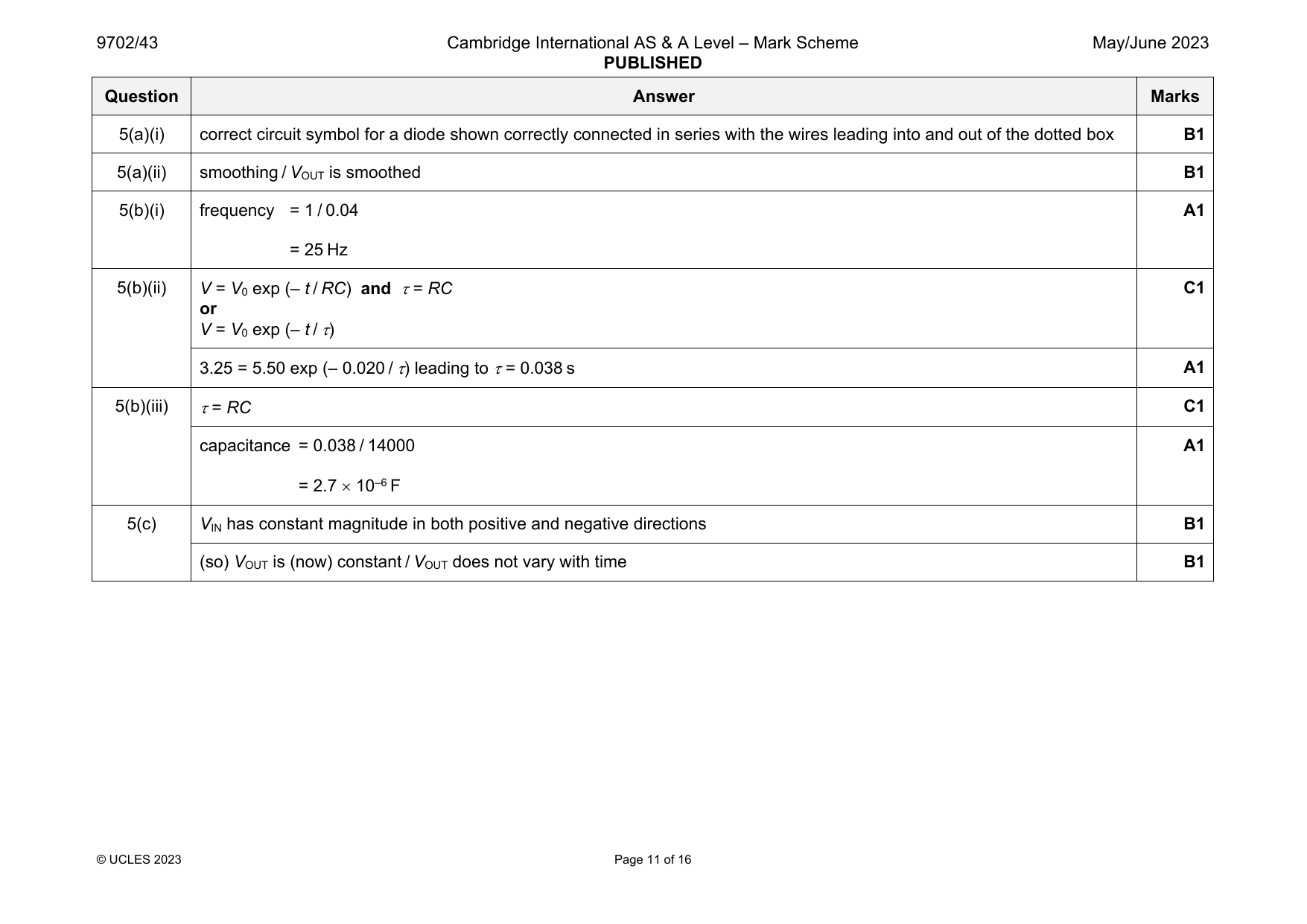
May/June 2023 · Paper 43 · Question 5 · 9 marks
5(a)(i) correct circuit symbol for a diode shown correctly connected in series with the wires leading into and out of the dotted box B1
5(a)(ii) smoothing / V is smoothed B1
OUT
5(b)(i) frequency = 1 / 0.04 A1
= 25 Hz
5(b)(ii) V = V exp (– t / RC) and = RC C1
0
or
V = V exp (– t / )
0
3.25 = 5.50 exp (– 0.020 / ) leading to = 0.038 s A1
5(b)(iii) = RC C1
capacitance = 0.038 / 14000 A1
= 2.7 10–6 F
5(c) V has constant magnitude in both positive and negative directions B1
IN
(so) V is (now) constant / V does not vary with time B1
OUT OUT
© UCLES 2023 Page 11 of 16
Official mark scheme pages: 11 · source PDF URL
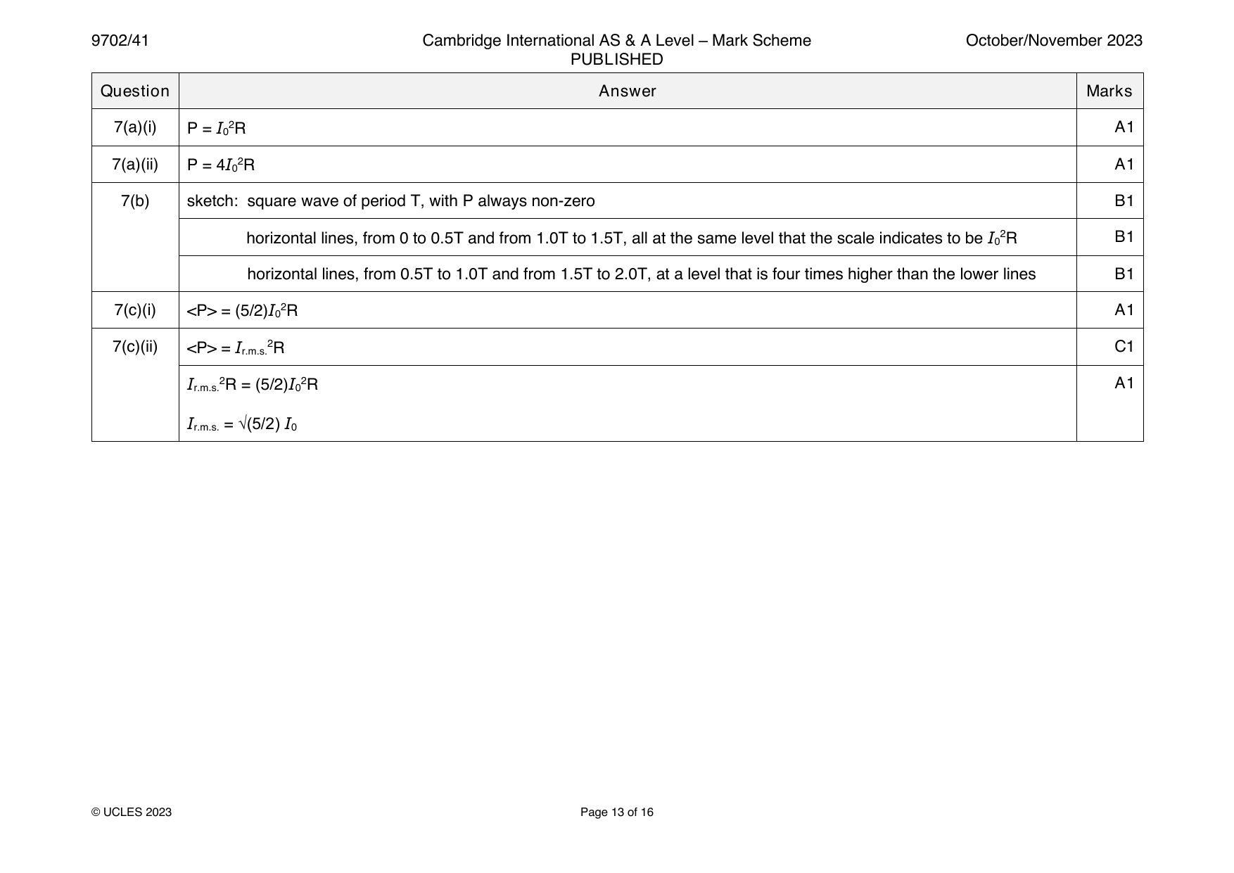
9702-2023-on-41-q07
Oct/Nov 2023 · Paper 41 · Question 7 · 8 marks
7(a)(i) P = I 2R A1
0
7(a)(ii) P = 4I 2R A1
0
7(b) sketch: square wave of period T, with P always non-zero B1
horizontal lines, from 0 to 0.5T and from 1.0T to 1.5T, all at the same level that the scale indicates to be I 2R B1
0
horizontal lines, from 0.5T to 1.0T and from 1.5T to 2.0T, at a level that is four times higher than the lower lines B1
7(c)(i) <P> = (5/2)I 2R A1
0
7(c)(ii) <P> = I 2R C1
r.m.s.
I 2R = (5/2)I 2R A1
r.m.s. 0
I = √(5/2) I
r.m.s. 0
© UCLES 2023 Page 13 of 16
Official mark scheme pages: 13 · source PDF URL
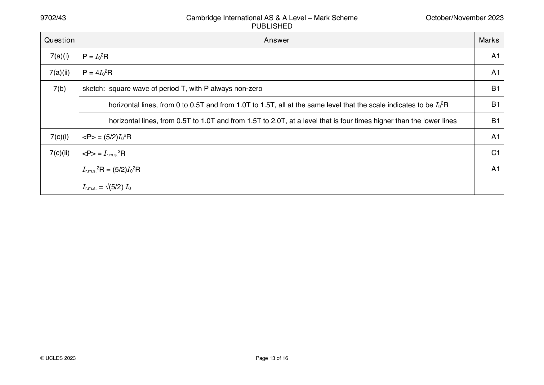
9702-2023-on-43-q07
Oct/Nov 2023 · Paper 43 · Question 7 · 8 marks
7(a)(i) P = I 2R A1
0
7(a)(ii) P = 4I 2R A1
0
7(b) sketch: square wave of period T, with P always non-zero B1
horizontal lines, from 0 to 0.5T and from 1.0T to 1.5T, all at the same level that the scale indicates to be I 2R B1
0
horizontal lines, from 0.5T to 1.0T and from 1.5T to 2.0T, at a level that is four times higher than the lower lines B1
7(c)(i) <P> = (5/2)I 2R A1
0
7(c)(ii) <P> = I 2R C1
r.m.s.
I 2R = (5/2)I 2R A1
r.m.s. 0
I = √(5/2) I
r.m.s. 0
© UCLES 2023 Page 13 of 16
Official mark scheme pages: 13 · source PDF URL
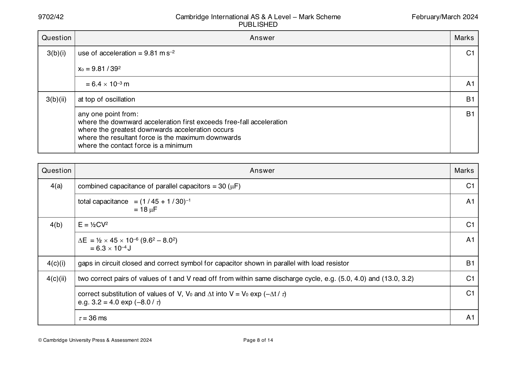
9702-2024-m-42-q04
March 2024 · Paper 42 · Question 4 · 10 marks
4(a) combined capacitance of parallel capacitors = 30 (F) C1
total capacitance = (1 / 45 + 1 / 30)–1 A1
= 18 F
4(b) E = ½CV2 C1
E = ½ 45 10–6 (9.62 – 8.02) A1
= 6.3 10–4 J
4(c)(i) gaps in circuit closed and correct symbol for capacitor shown in parallel with load resistor B1
4(c)(ii) two correct pairs of values of t and V read off from within same discharge cycle, e.g. (5.0, 4.0) and (13.0, 3.2) C1
correct substitution of values of V, V and t into V = V exp (–t / ) C1
0 0
e.g. 3.2 = 4.0 exp (–8.0 / )
= 36 ms A1
© Cambridge University Press & Assessment 2024 Page 8 of 14
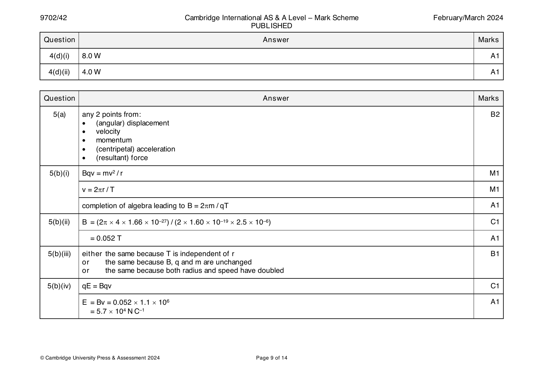
4(d)(i) 8.0 W A1
4(d)(ii) 4.0 W A1
Question Answer Marks
Official mark scheme pages: 8, 9 · source PDF URL
9702-2024-mj-41-q07
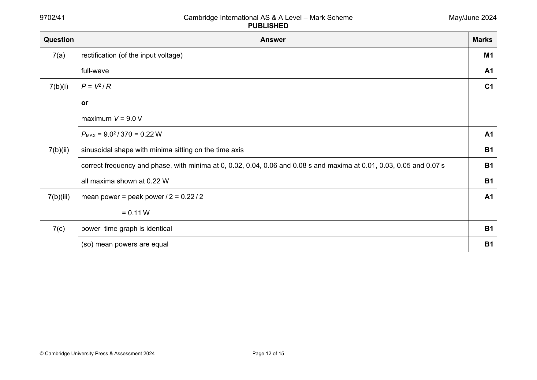
May/June 2024 · Paper 41 · Question 7 · 10 marks
7(a) rectification (of the input voltage) M1
full-wave A1
7(b)(i) P = V2 / R C1
or
maximum V = 9.0 V
P = 9.02 / 370 = 0.22 W A1
MAX
7(b)(ii) sinusoidal shape with minima sitting on the time axis B1
correct frequency and phase, with minima at 0, 0.02, 0.04, 0.06 and 0.08 s and maxima at 0.01, 0.03, 0.05 and 0.07 s B1
all maxima shown at 0.22 W B1
7(b)(iii) mean power = peak power / 2 = 0.22 / 2 A1
= 0.11 W
7(c) power–time graph is identical B1
(so) mean powers are equal B1
© Cambridge University Press & Assessment 2024 Page 12 of 15
Official mark scheme pages: 12 · source PDF URL
9702-2024-mj-43-q07
May/June 2024 · Paper 43 · Question 7 · 10 marks
7(a) rectification (of the input voltage) M1
full-wave A1
7(b)(i) P = V2 / R C1
or
maximum V = 9.0 V
P = 9.02 / 370 = 0.22 W A1
MAX
7(b)(ii) sinusoidal shape with minima sitting on the time axis B1
correct frequency and phase, with minima at 0, 0.02, 0.04, 0.06 and 0.08 s and maxima at 0.01, 0.03, 0.05 and 0.07 s B1
all maxima shown at 0.22 W B1
7(b)(iii) mean power = peak power / 2 = 0.22 / 2 A1
= 0.11 W
7(c) power–time graph is identical B1
(so) mean powers are equal B1
© Cambridge University Press & Assessment 2024 Page 12 of 15
Official mark scheme pages: 12 · source PDF URL
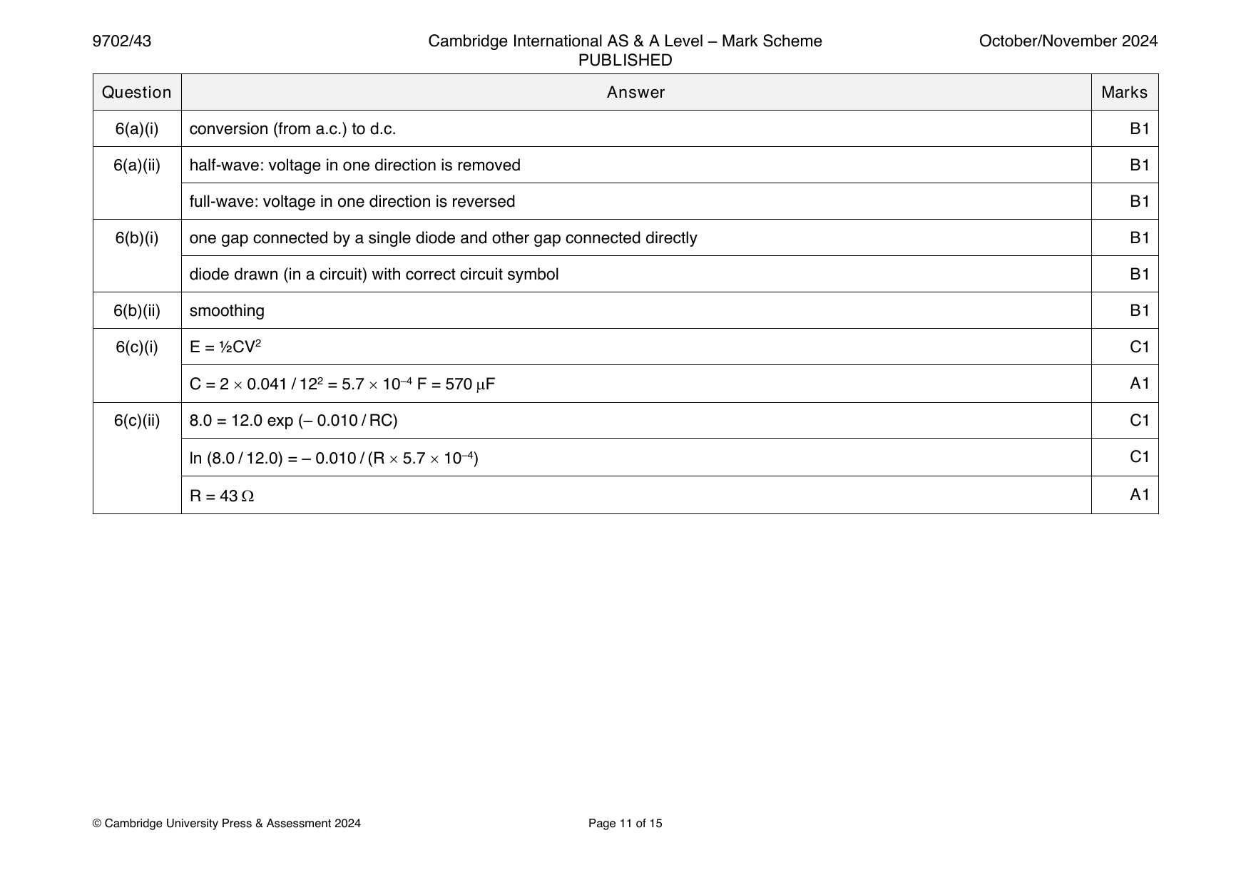
9702-2024-on-41-q06
Oct/Nov 2024 · Paper 41 · Question 6 · 11 marks
6(a)(i) conversion (from a.c.) to d.c. B1
6(a)(ii) half-wave: voltage in one direction is removed B1
full-wave: voltage in one direction is reversed B1
6(b)(i) one gap connected by a single diode and other gap connected directly B1
diode drawn (in a circuit) with correct circuit symbol B1
6(b)(ii) smoothing B1
6(c)(i) E = ½CV2 C1
C = 2 0.041 / 122 = 5.7 10–4 F = 570 F A1
6(c)(ii) 8.0 = 12.0 exp (– 0.010 / RC) C1
ln (8.0 / 12.0) = – 0.010 / (R 5.7 10–4) C1
R = 43 A1
© Cambridge University Press & Assessment 2024 Page 11 of 15
Official mark scheme pages: 11 · source PDF URL
9702-2024-on-42-q08
Oct/Nov 2024 · Paper 42 · Question 8 · 9 marks
8(a) number of cycles per unit time B1
8(b)(i) period = 2 / 40 = 0.050 s = 50 ms A1
8(b)(ii) sinusoidal curve, starting at (0, 0) and initially increasing from there B1
periodic line showing 2 cycles with period 50 ms from t = 0 to t = 100 ms B1
all peaks shown at I = +3.5 A and all troughs shown at I = –3.5 A B1
8(b)(iii) I = 3.5 / √2 A1
r.m.s
= 2.5 A
8(c) P = I2R C1
peak power = 3.52 680 (= 8330 W) M1
or
mean power = 2.472 680 (= 4170 W)
peak and mean powers both calculated correctly, with supporting working, and compared leading to conclusion that mean A1
power is half the peak power
© Cambridge University Press & Assessment 2024 Page 12 of 14
Official mark scheme pages: 12 · source PDF URL
9702-2024-on-43-q06
Oct/Nov 2024 · Paper 43 · Question 6 · 11 marks
6(a)(i) conversion (from a.c.) to d.c. B1
6(a)(ii) half-wave: voltage in one direction is removed B1
full-wave: voltage in one direction is reversed B1
6(b)(i) one gap connected by a single diode and other gap connected directly B1
diode drawn (in a circuit) with correct circuit symbol B1
6(b)(ii) smoothing B1
6(c)(i) E = ½CV2 C1
C = 2 0.041 / 122 = 5.7 10–4 F = 570 F A1
6(c)(ii) 8.0 = 12.0 exp (– 0.010 / RC) C1
ln (8.0 / 12.0) = – 0.010 / (R 5.7 10–4) C1
R = 43 A1
© Cambridge University Press & Assessment 2024 Page 11 of 15
Official mark scheme pages: 11 · source PDF URL
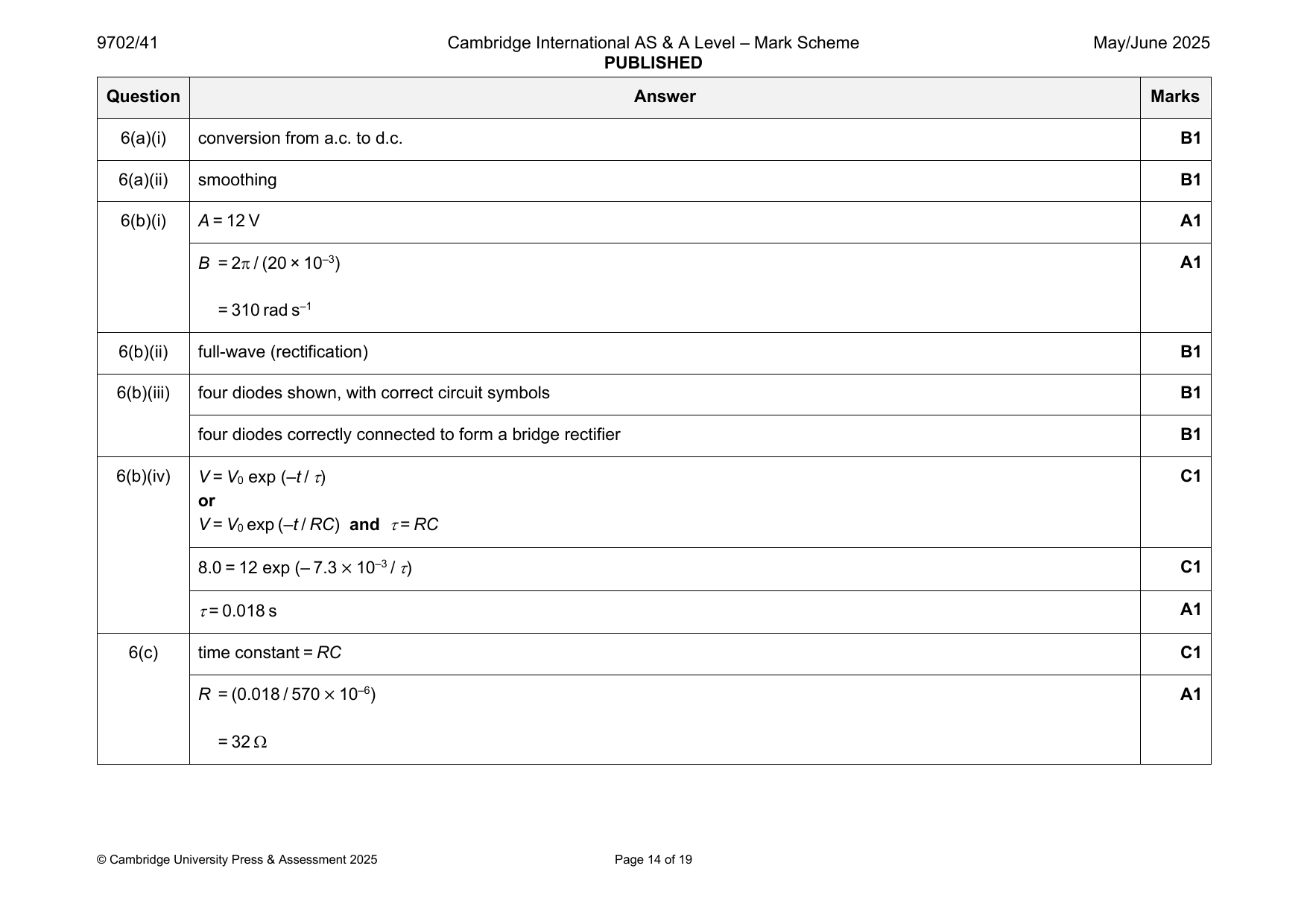
9702-2025-mj-41-q06
May/June 2025 · Paper 41 · Question 6 · 12 marks
6(a)(i) conversion from a.c. to d.c. B1
6(a)(ii) smoothing B1
6(b)(i) A = 12 V A1
B = 2 / (20 × 10–3) A1
= 310 rad s–1
6(b)(ii) full-wave (rectification) B1
6(b)(iii) four diodes shown, with correct circuit symbols B1
four diodes correctly connected to form a bridge rectifier B1
6(b)(iv) V = V exp (–t / ) C1
0
or
V = V exp (–t / RC) and = RC
0
8.0 = 12 exp (– 7.3 × 10⁻³ / ) C1
= 0.018 s A1
6(c) time constant = RC C1
R = (0.018 / 570 × 10–6) A1
= 32
© Cambridge University Press & Assessment 2025 Page 14 of 19
Official mark scheme pages: 14 · source PDF URL
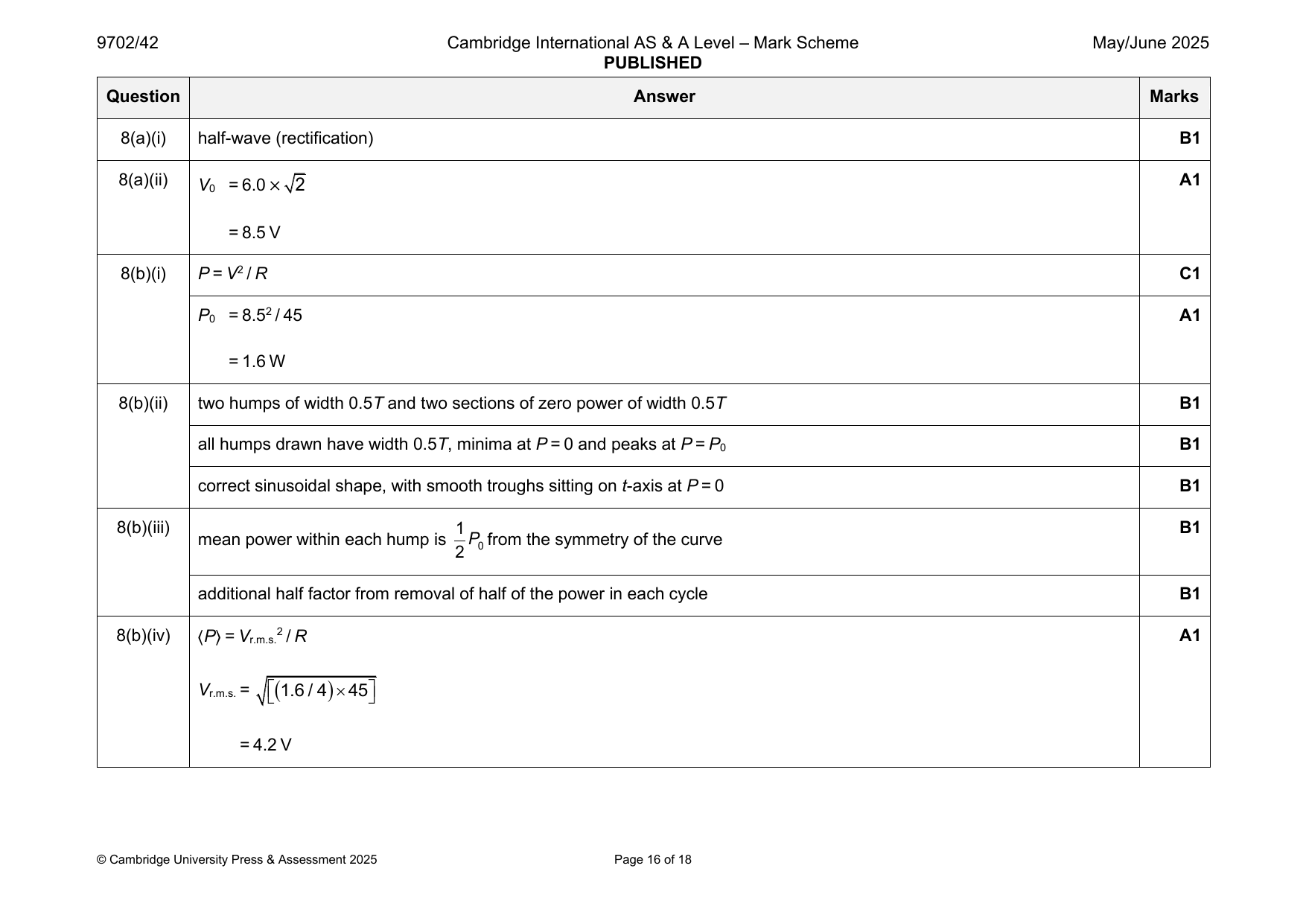
9702-2025-mj-42-q08
May/June 2025 · Paper 42 · Question 8 · 10 marks
8(a)(i) half-wave (rectification) B1
8(a)(ii) A1
V = 6.0 × 2
0
= 8.5 V
8(b)(i) P = V2 / R C1
P = 8.52 / 45 A1
0
= 1.6 W
8(b)(ii) two humps of width 0.5T and two sections of zero power of width 0.5T B1
all humps drawn have width 0.5T, minima at P = 0 and peaks at P = P B1
0
correct sinusoidal shape, with smooth troughs sitting on t-axis at P = 0 B1
8(b)(iii) 1 B1
mean power within each hump is P from the symmetry of the curve
2 0
additional half factor from removal of half of the power in each cycle B1
8(b)(iv) 〈P〉 = V 2 / R A1
r.m.s.
V = (1.6/4)45
r.m.s.
= 4.2 V
© Cambridge University Press & Assessment 2025 Page 16 of 18
Official mark scheme pages: 16 · source PDF URL
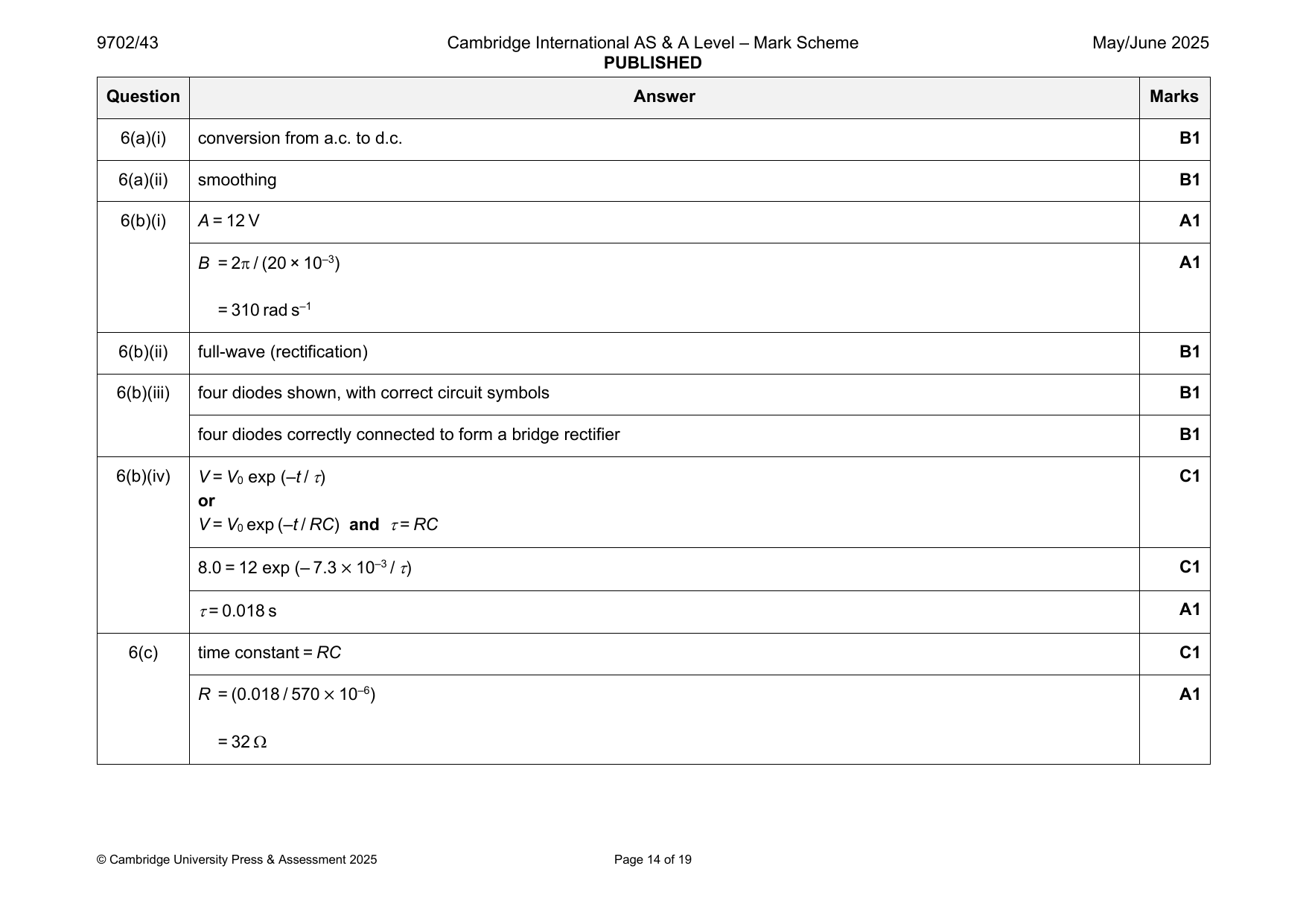
9702-2025-mj-43-q06
May/June 2025 · Paper 43 · Question 6 · 12 marks
6(a)(i) conversion from a.c. to d.c. B1
6(a)(ii) smoothing B1
6(b)(i) A = 12 V A1
B = 2 / (20 × 10–3) A1
= 310 rad s–1
6(b)(ii) full-wave (rectification) B1
6(b)(iii) four diodes shown, with correct circuit symbols B1
four diodes correctly connected to form a bridge rectifier B1
6(b)(iv) V = V exp (–t / ) C1
0
or
V = V exp (–t / RC) and = RC
0
8.0 = 12 exp (– 7.3 × 10⁻³ / ) C1
= 0.018 s A1
6(c) time constant = RC C1
R = (0.018 / 570 × 10–6) A1
= 32
© Cambridge University Press & Assessment 2025 Page 14 of 19
Official mark scheme pages: 14 · source PDF URL
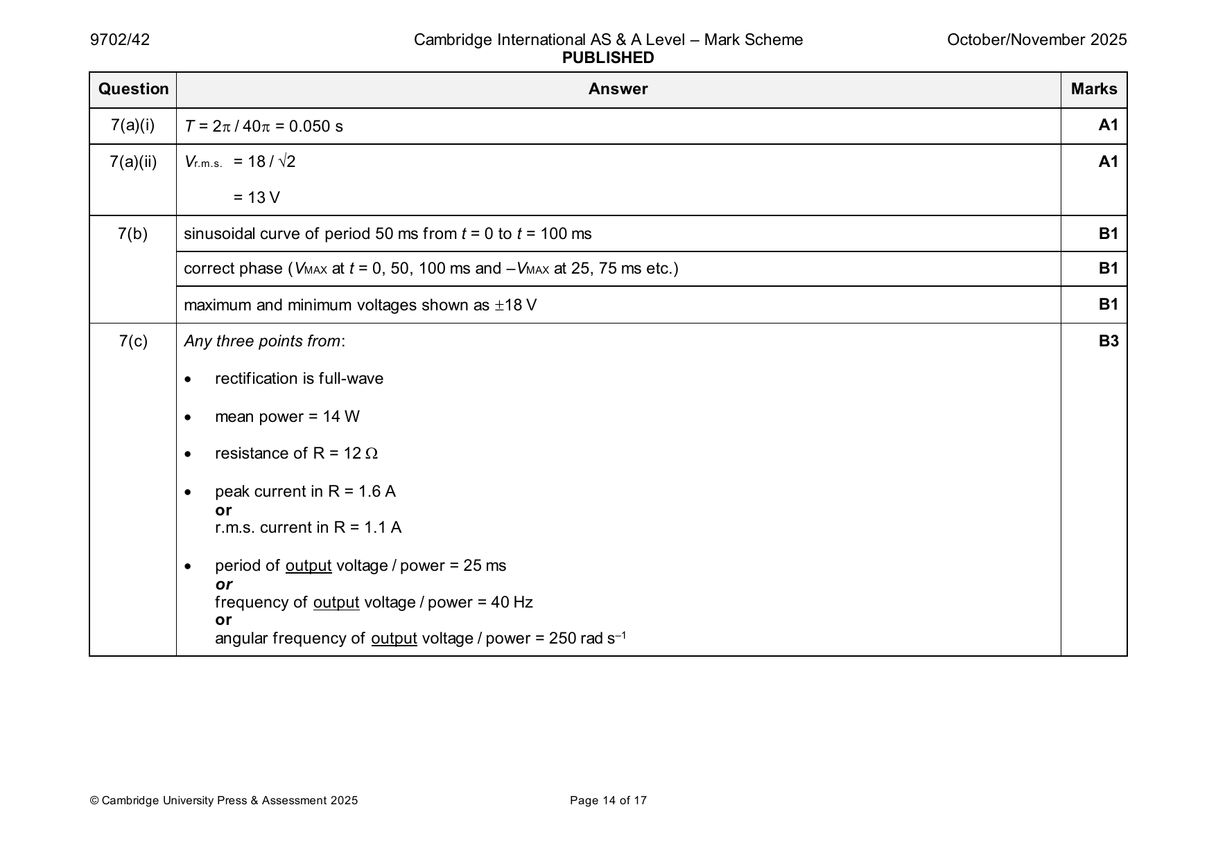
9702-2025-on-42-q07
Oct/Nov 2025 · Paper 42 · Question 7 · 8 marks
7(a)(i) T = 2 / 40 = 0.050 s A1
7(a)(ii) V = 18 / √2 A1
r.m.s.
= 13 V
7(b) sinusoidal curve of period 50 ms from t = 0 to t = 100 ms B1
correct phase (V at t = 0, 50, 100 ms and –V at 25, 75 ms etc.) B1
MAX MAX
maximum and minimum voltages shown as 18 V B1
7(c) Any three points from: B3
• rectification is full-wave
• mean power = 14 W
• resistance of R = 12
• peak current in R = 1.6 A
or
r.m.s. current in R = 1.1 A
• period of output voltage / power = 25 ms
or
frequency of output voltage / power = 40 Hz
or
angular frequency of output voltage / power = 250 rad s–1
© Cambridge University Press & Assessment 2025 Page 14 of 17
Official mark scheme pages: 14 · source PDF URL